94
7521
7521
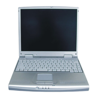
Plus / N N/B MAINTENANCE
Plus / N N/B MAINTENANCE
5. Pin Descriptions Of Major Components
5.2 SiS630S Slot 1/Socket 370 2D/3D Ultra-AGP™ Single Chipset
Power management Interface
Name Tolerance Power
Plane
Type
Attr
Description
THERM#
3.3V/5V MAIN I
Thermal Detect :
THERM# is connected to the
internal ACPI-compatible power management
unit as an indication of outstanding thermal event.
An active THERM# event can be used to generate
SCI/SMI#/GPEIRQ. If THERM# is activated for
more than 2 second, a thermal override event will
occur and the system will enter CPU thermal
throttling mode automatically.
GPIO[6:4]
3.3V/5V AUX I/O/OD General Purpose Input/Output [6:4]: Refer to GPIO
description.
SMBus Interface
Name Tolerance Power
Plane
Type
Attr
Description
SMBDAT
I2CDAT
3.3V/5V MAIN I/OD
I/OD
SMBus Data :
SMBus data input/output pin.
I2C Data :
I2C data input/output pin.
SMCLK
I2CCLK
3.3V/5V MAIN I/OD
I/OD
SMBus Clock :
SMBus clock input/output pin.
I2C Clock :
I2C clock input/output pin.
SMBALT#
I2CALT#
GPIO15
3.3V/5V AUX I/OD
I/OD
I/O/OD
SMBus Alert :
This pin is used for SMBus device to
wake up the system from sleep state or to generate
SCI/SMI#/GPEIRQ.
I2C Alert :
This pin is used for I2C device to wake
up the system from sleep state or to generate
SCI/SMI#/GPEIRQ.
General Purpose Input/Output 15 :
Refer to GPIO
description.
Keyboard controller Interface
Name Tolerance Power
Plane
Type
Attr
Description
KBDAT
GPIO10
3.3V/5V AUX I/OD
I/O/OD
Keyboard Dada :
When the internal keyboard
controller is enabled, this pin is used as the keyboard
data signal.
General Purpose Input/Output 10 :
Refer to GPIO
description.
KBCLK
GPIO11
3.3V/5V AUX I/OD
I/O/OD
Keyboard Clock :
When the internal keyboard
controller is enabled, this pin is used as the keyboard
clock signal. General Purpose Input/Output 11 :
Refer to GPIO description.
Name Tol erance Power
Plane
Ty p e
Attr
Descri pti on
PMDAT
GPI O12
3.3V/5V AUX I/OD
I/O/OD
PS2 Mouse Data:
When the internal keyboard and PS2 mouse controllers are
enabled, this pin is
used as PS2 mouse data signal.
General Purpose Input/Output 12 :
Refer to GPIO description.
PMCLK
GPI O13
3.3V/5V AUX I/OD
I/O/OD
PS2 Mouse Clock:
When the internal keyboard and PS2 mouse controllers are
enabled, this pin is used as the PS2 mouse clock signal.
General Purpose Input/Output 13 :
Refer to GPIO description.
KLOCK#
GPI O14
3.3V/5V AUX I
I/O/OD
Keyboard Lock:
When KLOCK# is tied low, the internal keyboard controller
will not respond to
any key-strikes.
General Purpose Input/Output 14 :
Refer to GPIO description.
LPC Interface
Name Tol erance Power
Plane
Ty p e
Attr
Description
LAD[3:0]
3.3V/5V MAIN I/O
LPC Address/Data Bus :
LPC controller drives these four pins to transmit LPC
command, address,
and data to LPC device.
LDRQ#
3.3V/5V MAIN I
LPC DMA Request 0:
This pin is used by LPC device to request DMA cycle.
LFRAME#
3.3V MAIN O
LPC Frame :
This pin is used to notify LPC device
that a start or a abort LPC cycle will occur.
SIRQ
3.3V/5V MAIN I/OD
Serial IRQ :
This signal is used as the serial IRQ
line signal.