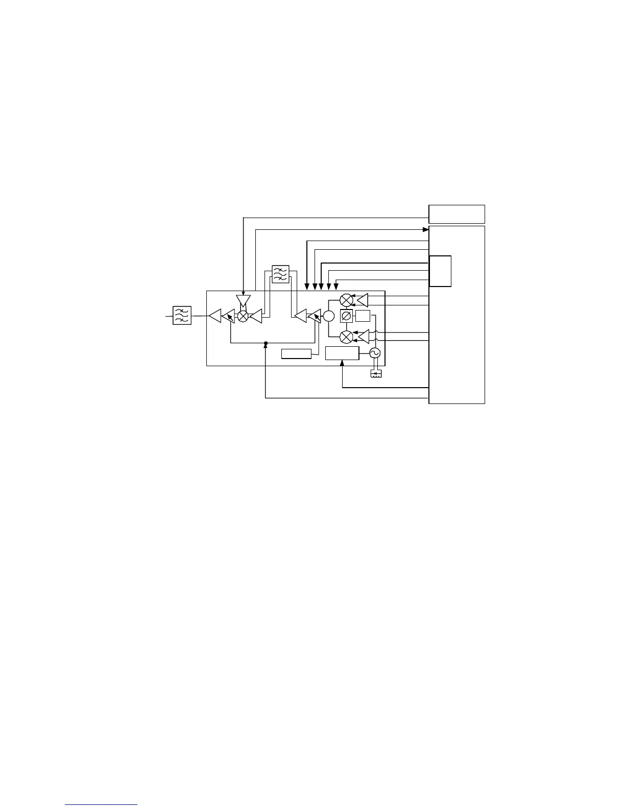
A920: TX Modulator (MAX2363)
Description
The in phase (I) and quadrature phase (Q) inputs are received at pins #23 (Q+), #24(Q-), #25(I+), & #26(I-) of U200. The expected DC bias levels are 1.30V - 1.40V
with a minimum 300mVpp signal upon the DC level.
The MAX2363 receives the differential I/Q BaseBand input and converts it up to the IF frequency of 380MHz through a quadrature modulator and IF variable gain
amplifier (VGA). The IFINH+ (pin #10) and IFINH- (pin #11) input are connected through off-chip FL201 from IFOUT+ (pin #17) and IFOUT- (pin #16), respectively.
The function of FL201 is to provide image rejection and out-of-band interferers filtering. The frequency conversion process performed by the mixer / oscillator combina-
tion sometimes will allow a frequency other than desired frequency to be fed into the IF and subsequently amplified. The SAW filter (FL201) has a nominal center fre-
quency of 380MHz and an insertion loss of ~ 3.5dB with a total bandwidth of 5MHz.
The IF and RF VGA (VGC1) are common and allow for varying the IF / RF output level . HARMONY_LITE controls the VGC signal with a range of ~1.3 - 2.6V and
provides gain a control range of ~75dB.
The MAX2363 VCO output frequency is controlled by an internal phase lock loop (PLL) synthesizer. The external loop filter consists of the components connected to
pins #33 and #32 (& pin #38). The VCO output frequency (TankH+ / TankH-) at pin #33and pin #32 are divided down internally, to a desired comparison frequency.
The reference signal at pin #36 (REF_FREQ) is also divided down to the same comparison frequency. The two divided signals are then compared with a three state digi-
tal phase detector. The internal phase detector drives the charge pump as well as the lock-detect logic(2361_LOCK). The charge pump output (IFCP, pin # 38) is pro-
cessed by the external loop filter and drives the tunable resonant network, altering the VCO frequency (760MHz) and closing the loop.
The differential IF output at pins #17 & #16 (IFOUTH+ / IFOUTH-) support high IF operation of frequency of 380MHz. The signal is routed to an off-chip IF SAW filter
(FL201) and up-mixed to RF through an image reject mixer and RF VGA. The signal is further amplified with an on-chip PA driver. The RF signal is then routed to an
interstage RF SAW filter (FL401).
The IF synthesizer (760 MHz VCO) and local oscillator (RF_LO) buffer are both programmable through the 3-wire bus. The sequence manager from HARMONY_LITE
programs standby mode(TX_STBY*) and shutdown mode(2361_SHDN). This IC operates from a pair of supply voltages VCC_DIG (isolated supply for IF_CP and 760
VCO) & VCC_ANA derived from VRF_TX_2_775V.
Motorola Confidential Proprietary
4-28
¸
2
380 MHz
Offset
Synthesizer
MAX2363
U200
/2
IF PLL
Σ
IF SAW
FL201
TX SAW
FL401
1920-1980MHz
IF Gain
760 MHz
VGC1
TX_I+
TX_I-
TX_Q+
TX_Q-
ASPI_CLK
ASPI_DATA
2361_CS
REF_FREQ
TX_LO
2361_SHDN
TX_STBY*
2361_LOCK
Harmony Lite
U101
SPI
FL150
 Loading...