Do you have a question about the NAD T 741 and is the answer not in the manual?
Instructions for replacing fuses with the correct type to prevent fire risk.
Procedures for safety checks, including leakage current measurements, before returning the unit.
Technical specifications for the power and preamplifier stages, including distortion and sensitivity.
Technical specifications for surround sound processing, including channel separation and frequency response.
Technical specifications for DTS audio decoding.
Technical specifications for the AM tuner functionality, including sensitivity and selectivity.
Technical specifications for the FM tuner functionality, including sensitivity and signal-to-noise ratio.
Electrical power consumption and requirements for European and North American models.
Dimensions and weight of the unit.
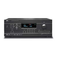
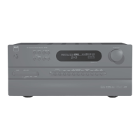
Description of connectors and controls located on the rear panel of the unit.
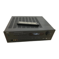
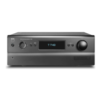
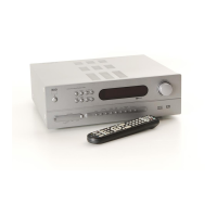
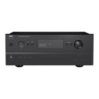
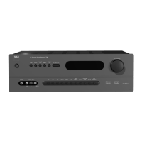
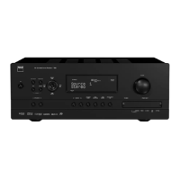
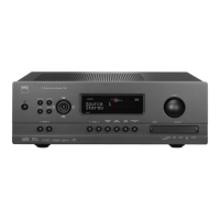
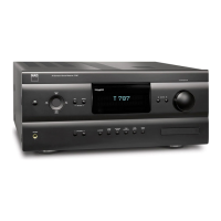
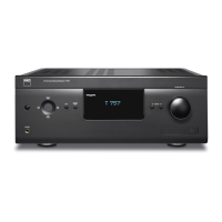
Description of controls, indicators, and connectors on the front panel.
Step-by-step guide for removing screws from side and back panels during disassembly.
Instructions for safely detaching the top cover assembly from the unit.
Diagram showing adjustment points for the tuner section.
Diagram showing adjustment points for idle current on amplifier boards.
Setup configuration for measuring FM signal parameters.
Setup configuration for measuring Radio Data System (RDS) signals.
Setup configuration for measuring AM signal parameters.
Procedures for aligning amplifier section parameters.
Specific steps for setting the idle current in amplifier channels.
Component layout diagram for the S-Video processing board.
Component layout diagram for the Surround Amplifier board.
Component layout diagram for the Video board.
Component layout on the solder side of the Multi-channel board.
Component layout on the component side of the Multi-channel board.
Component layout on the component side of the AC3 board.
Component layout diagram for the Key board.
Component layout diagram for the Video-5 input board.
Component layout diagram for the Primary circuit board.
Component layout diagram for the Tuner board.
Component layout on the solder side of the AC3 board.
Component layout diagram for the Power Switch board.
Component layout diagram for the volume control board.
Component layout diagram for the Secondary circuit board.
Component layout diagram for the LED indicator board.
Schematic diagram for AC3 and DTS processing circuits.
Schematic diagram for the main processing board.
Schematic diagram for the multi-channel audio processing.
Schematic diagram for the Key board interface.
Schematic diagram for the Tuner section.
Schematic diagram for the S-Video input/output circuits.
Schematic diagram for the front amplifier stage.
Schematic diagram for the audio processing circuits.
Schematic diagram for the video processing circuits.
Schematic diagram for the surround amplifier stage.
Schematic diagram for the Power Supply Unit.
Block diagram of the CS4926 IC on the AC3 board.
Block diagram of the CS8414 IC on the AC3 board.
Block diagram of CS4340 ICs on the AC3 board.
Block diagram of LC87F65C8A IC on the Key board.
Block diagram of NJM5532M IC on the Main board.
Block diagram of M6244FP IC on the Multi-channel board.
Block diagram of LA1837 IC on the Tuner board.
Block diagram of LC72723M IC on the Tuner board.
List of electrical components for the AC3 board.