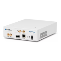
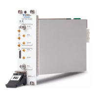
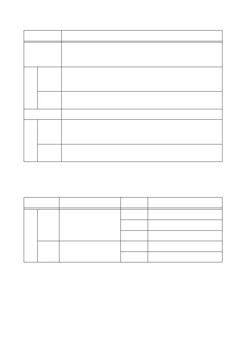
Table 2. Connector Descriptions
Pin Description
JTAG A USB port that connects the host computer to the device FPGA for
development and debugging. LabVIEW FPGA does not currently support
configuring or programming the device FPGA using the JTAG connector.
RF 0 TX1 RX1 Input and output terminal for the RF signal. TX1 RX1 is an SMA (f)
connector with an impedance of 50 Ω and is a single-ended input or output
channel.
RX2 Input terminal for the RF signal. RX2 is an SMA (f) connector with an
impedance of 50 Ω and is a single-ended input channel.
AUX I/O General-purpose I/O (GPIO) port. AUX I/O is controlled by the FPGA.
RF 1 TX1 RX1 Input and output terminal for the RF signal. TX1 RX1 is an SMA (f)
connector with an impedance of 50 Ω and is a single-ended input or output
channel.
RX2 Input terminal for the RF signal. RX2 is an SMA (f) connector with an
impedance of 50 Ω and is a single-ended input channel.
The LED indications described in the following table occur only when you use the NI-USRP
API with the default FPGA image. When you use LabVIEW FPGA, you customize the LED
indications.
Table 3. LED Descriptions
Pin Description Color Indication
RF 0 TX1
RX1
Indicates the transmit
status of the device.
Off The device is not active.
Red The device is receiving data.
Green The device is transmitting data.
RX2 Indicates the receive status
of the device.
Off The device is not receiving data.
Green The device is receiving data.
16 | ni.com | USRP-2950/2952/2953/2954/2955 Getting Started Guide
 Loading...