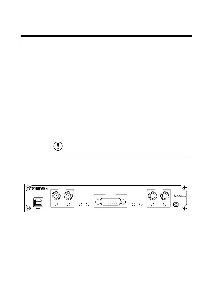
Table 10. Connector Descriptions (Continued)
Connector Use
PCIe x4 Port for a PCI Express Generation 1, x4 bus connection through an MXI
Express four-lane cable.
PPS TRIG
OUT
Output terminal for the pulse per second (PPS) timing reference. PPS TRIG
OUT is a female SMA connector with an impedance of 50 Ω, and it is a
single-ended input. The output signal is 0 V to 3.3 V TTL. You can also use
this port as triggered output (TRIG OUT) that you program with the PPS
Trig Out I/O signal.
PPS TRIG IN Input terminal for pulse per second (PPS) timing reference. PPS TRIG IN
is a female SMA connector with an impedance of 50 Ω, and it is a single-
ended input channel. PPS TRIG IN accepts 0 V to 3.3 V TTL and 0 V to
5 V TTL signals. You can also use this port as a triggered input (TRIG IN)
that you control using NI-USRP software.
GPS ANT Input terminal for the GPS antenna signal. GPS ANT is a female SMA
connector with a maximum input power of -15 dBm and an output of
DC 5 V to power an active antenna.
Notice Do not terminate the GPS ANT port if you do not use
it.
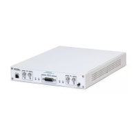
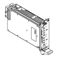
USRP-2954 Front Panel, Back Panel, and LEDs
Front Panel
LINK
TX OUTPUT MAX +20 dBm, RX INPUT MAX -15 dBm, ALL RF PORTS 50 Ω
TX1 RX1 RX2GPSPPSREF
TX1 RX1 RX2
RF 0 RF 1
JTAG
AUX I/O
3.3 VDC MAX
Designed by Ettus Research
PWR
NI USRP-2954R
10 MHz - 6 GHz, GPS-Disciplined Clock (160 MHz BW)
26 | ni.com | USRP-2950/2952/2953/2954/2955 Getting Started Guide