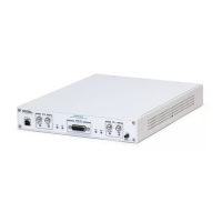
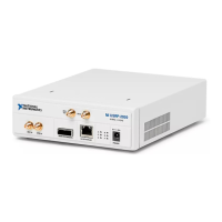
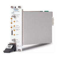
USRP-2953 Front Panel, Back Panel, and LEDs
Front Panel
LINK
TX OUTPUT MAX +20 dBm, RX INPUT MAX -15 dBm, ALL RF PORTS 50 Ω
TX1 RX1 RX2GPSPPSREF
TX1 RX1 RX2
RF 0 RF 1
JTAG
AUX I/O
3.3 VDC MAX
NI USRP-2953R
1.2 GHz - 6 GHz
NI USRP-2953R
1.2 GHz - 6 GHz
PWR
Table 8. Connector Descriptions
Connector Use
JTAG A USB port that connects the host computer to the device FPGA for
recovery purposes. This port can be used with the Xilinx iMPACT
configuration tool to temporarily load a new bitfile.
RF 0 TX1 RX1 Input and output terminal for the RF signal. TX1 RX1 is an SMA (f)
connector with an impedance of 50 Ω and is a single-ended input or output
channel.
RX2 Input terminal for the RF signal. RX2 is an SMA (f) connector with an
impedance of 50 Ω and is a single-ended input channel.
AUX I/O General-purpose I/O (GPIO) port. AUX I/O is controlled by the FPGA.
RF 1 TX1 RX1 Input and output terminal for the RF signal. TX1 RX1 is an SMA (f)
connector with an impedance of 50 Ω and is a single-ended input or output
channel.
RX2 Input terminal for the RF signal. RX2 is an SMA (f) connector with an
impedance of 50 Ω and is a single-ended input channel.
Note The LED indications described in the following table occur only when you
use the NI-USRP API with the default API image. When you use LabVIEW FPGA,
you customize the LED indications.
USRP-2950/2952/2953/2954/2955 Getting Started Guide | © National Instruments | 23