Hardware description
Note: No protection diodes are implemented. Make sure to connect the positive voltage to the pin
next to the “+” and GND to the pin next to “−“.
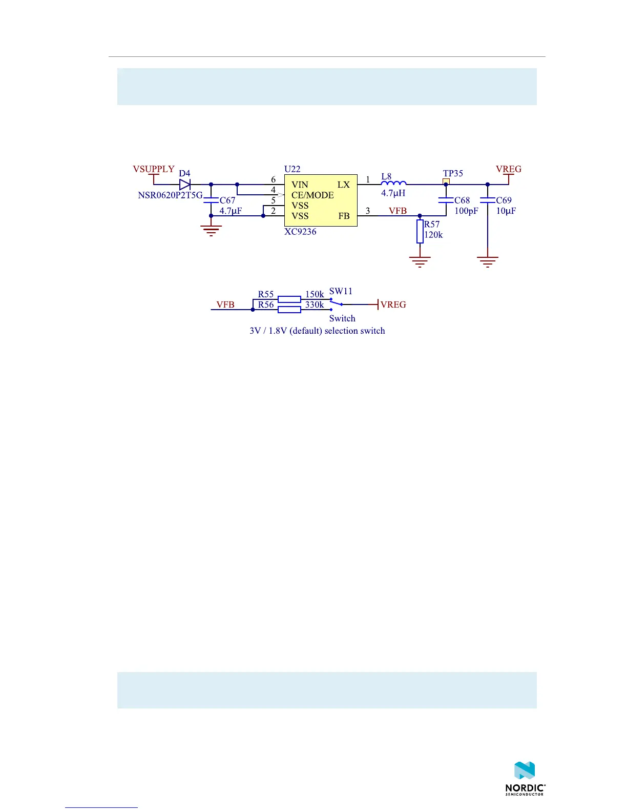
5.3.2 VDD supply rail
VDD is the main supply for the rest of the circuitry on the board. It is regulated down from VSUPPLY by a
buck regulator (U22).
Figure 11: VDD buck regulator and selection switch
You can set the VDD voltage to 1.8 V (default) or 3 V with SW11. Running 3 V GPIO with heavy load may
degrade the LTE RF performance. For more information, see GPIO - General purpose input/output in the
nRF9160 Objective Product Specification.
VDD powers most of the other circuits the board and will set the GPIO signal amplitude between nRF9160
and other circuits on the board including connectors and PIN headers.
5.3.3 Other power domains
The interface MCU needs a 3.3 V for its USB interface supply, a low-dropout voltage regulator (U32) is used
for this. This regulator also supplies the LEDs on the board, giving these a fixed supply.
5.4 Antenna interfaces
nRF9160 DK has three antenna interfaces mounted representing LTE, GPS, and the 2.4 GHz radio.
The RF signals are propagated through three coaxial connectors with switches that will disconnect the
corresponding antenna from the radio if adapter cables are connected. This makes it possible to perform
conducted measurements or attach external antennas to the radio.
The relation between the switches, radios, and antennas are the following:
• J1 – Switch between the nRF9160 and the LTE antenna (A1)
• J6 – Switch between the nRF9160 and the GPS antenna (A2)
• J7 – Switch between the nRF52840 and the 2.4 GHz antenna (A3)
Note: The GPS signal is RX only. There is a combined Low-Noise Amplifier (LNA) and a Band-Pass
Filter (BPF) (U3) between the nRF9160 and the RF switch J6.
4418_1216 v0.7
16
 Loading...