Hardware description
To utilize the SW trace feature on nRF9160, a footprint for a 20-pin connector is available (P4). If trace
functionality is required, a 2×10 pin 1.27 mm pitch surface mount connector can be mounted. nRF9160
GPIOs used for the trace interface will not be available for application firmware use during trace.
Note: Connectors P3 and P4 overlap and share the same footprint.
GPIO Trace
P0.21 TRACECLK
P0.22 TRACEDATA[0]
P0.23 TRACEDATA[1]
P0.24 TRACEDATA[2]
P0.25 TRACEDATA[3]
Table 6: nRF9160 trace interfaces
5.9.1 Debug output
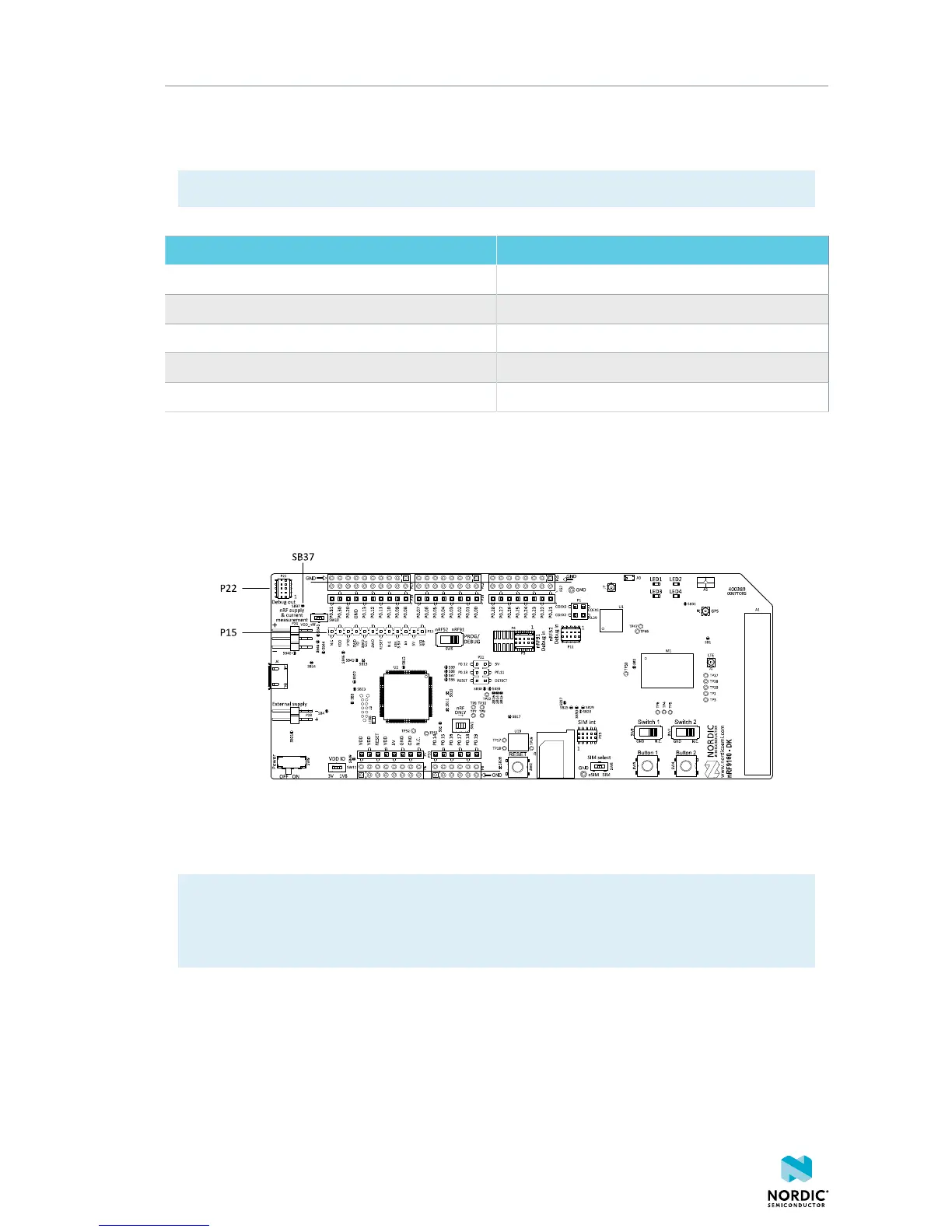
The nRF9160 DK board supports programming and debugging external boards with Nordic SoCs and SiPs.
To debug an external board with SEGGER J-Link OB IF, connect to the Debug out connector P22 to your
target board with a 10-pin flat cable.
Figure 20: Debug output connector
When the external board is powered, the interface MCU will detect the supply voltage of the board and
program/debug the target chip on the external board instead of the onboard nRF9160 and/or nRF52840.
Note: The voltage supported by external debugging/programming is the VDD voltage. This voltage
can be selected to 1.8 V or 3 V using slide switch SW11. For optimal performance of the nRF9160
radio, it is recommended that only 1.8 V is used. Make sure the voltage level of the external board
matches the VDD of the nRF9160 DK.
P15 can also be used as a debug out connector to program shield-mounted targets. For both P22 and P15,
the interface MCU will detect the supply voltage on the mounted shield and program/debug the target.
If the interface MCU detects target power on both P22 and P15, it will program/debug the target
connected to P22 by default.
If it is inconvenient to have a separate power supply on the external board, the nRF9160 DK can supply
power through the Debug out connector P22. To enable this, short solder bridge SB43.
4418_1216 v0.7
24
 Loading...