Hardware description
DestinationName nRF52 switch
control
Source
nRF9160
Default
1
Optional
P0.26 RTS P27 6
P0.27 CTS P27 7
P0.28 TX P27 8
nRF91_APP1 P1.14
P0.29
Interface
MCU VCOM0
RX P1 4
P1.12
(P0.12; see
footnote)
P0.01 P14 2 RXD
P0.00 P14 1 TXD
P0.15 P10 2 RTS
nRF91_APP2
P0.14 P10 1
Interface
MCU VCOM2
CTS
nRF91_LED1 P1.05 P0.02 - LED1 P14 3
nRF91_LED2 P1.07 P0.02 - LED2 P14 4
nRF91_LED3 P1.01 P0.02 - LED3 P14 5
nRF91_LED4 P1.03 P0.02 - LED4 P14 6
nRF91_SWITCH1 P1.09 P0.08 - SWITCH1 P19 1
nRF91_SWITCH2 P0.08 P0.09 - SWITCH2 P19 2
nRF91_BUTTON1 P0.06 P0.06 - BUTTON1 P14 7
nRF91_BUTTON2 P0.26 P0.07 - BUTTON2 P14 8
P0.17 P10 4 P0.17
P0.18 P10 5 P0.20
nRF91_GPIO P0.13
P0.19 P10 6
nRF52
P0.15
P0.21 P4 TRACECLK P0.22
P0.22 TRACEDATA0 P1.04
NRF91_TRACE P0.24
P0.23 TRACEDATA1
nRF52
P1.02
COEX0 COEX0_PH P1.13
COEX1 COEX1_PH P1.11
NRF91_COEX P1.10
COEX2
P1
COEX2_PH
nRF52
P1.15
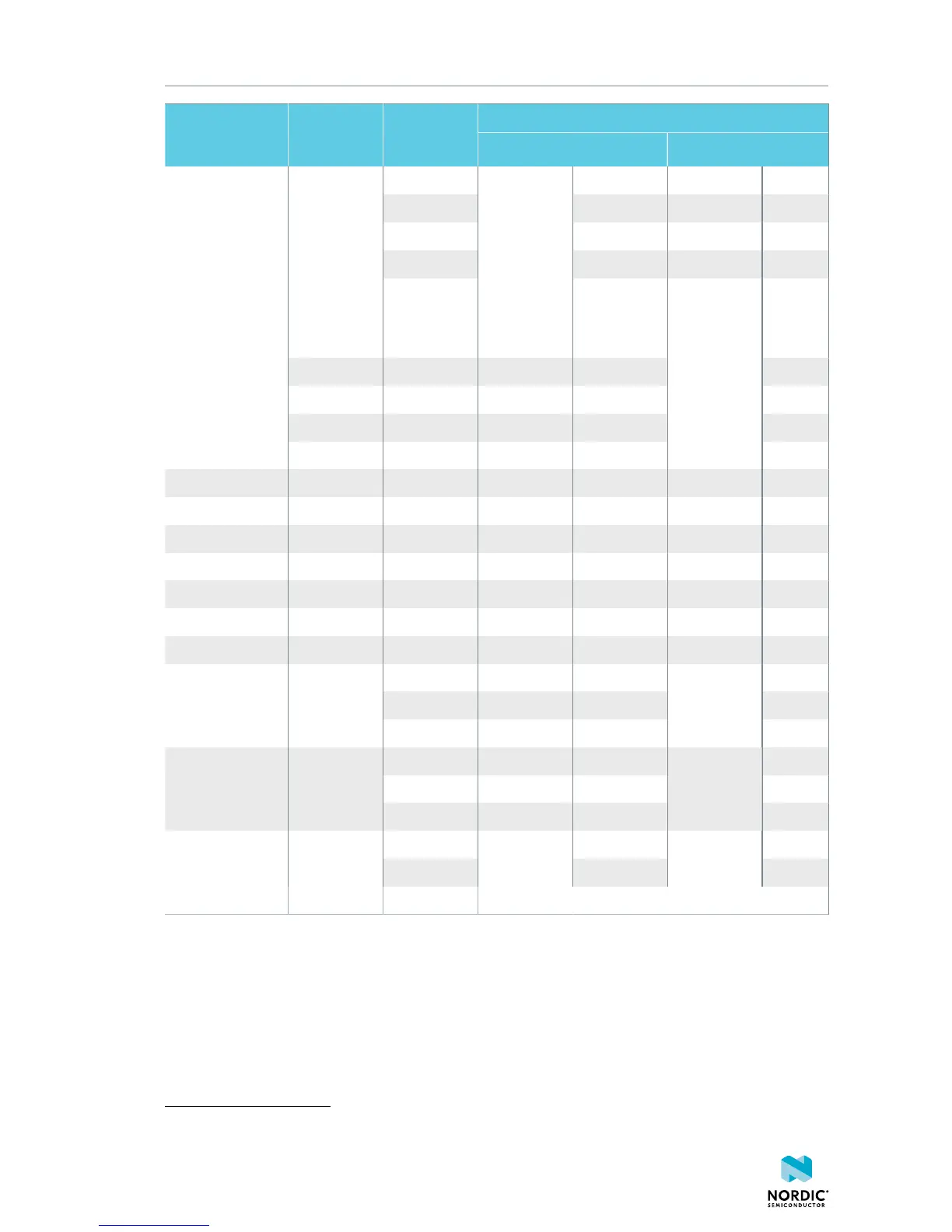
Table 4: Board control routing
Name
The name to be used when referring to this signal path and the configuration needed to control it.
nRF52 switch control
The GPIOs on nRF52840 that are used to control the analog switches selecting between default and
optional routing.
1
For nRF91_APP2, two GPIOs need to be set high on nRF52840 to get the optional destination for the
signals.
4418_1216 v0.7
20
 Loading...