USB and PCIe
PRELIMINARY INFORMATION
Jetson Orin NX Series and Jetson Orin Nano Series DG-10931-001_v1.1 | 37
Notes:
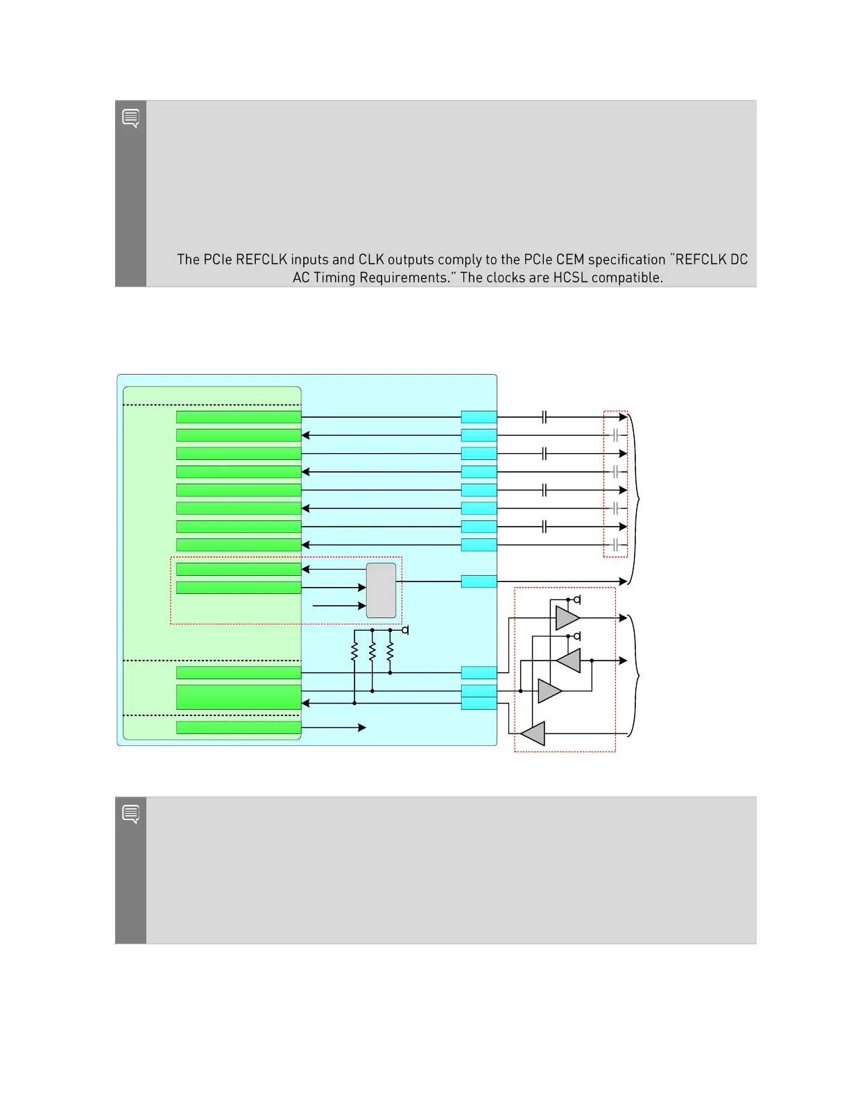
1. For Root Port operation, the mux should be set to output the SF_PCIE10_CLK signals. SoC
GP21 which is used for the mux select should be set low.
2. AC Capacitors required on RX lines on carrier board if connected directly to device. They
should not be on the carrier board if connected to PCIe connector, M.2 Key M, etc. In those
cases, the AC caps are on the board connected to those connectors.
3. See design guidelines for correct AC capacitor values.
4.
Specifications and
Figure 7-6 shows the x4 interface configured as Endpoint for the PCIe Endpoint connections.
Figure 7-6. PCIe Endpoint Connections Example
Jetson
SoC - PCIe
UPHY0
GP185_PCIE_WAKE_N
PEX
Ctrl
PCIe 0 Lane 3
PCIe 0 Lane 2
PCIe 0 Lane 1
PCIe 0 Lane 0
PCIE0_TX3_N/P
PCIE0_RX3_N/P
PCIE0_TX2_N/P
PCIE0_RX2_N/P
PCIE0_TX1_N/P
PCIE0_RX1_N/P
PCIE0_TX0_N/P
PCIE0_RX0_N/P
PCIE0_CLK_N/P
PCIE_WAKE*
PCIE0_CLKREQ*
PCIE0_RST*
3.3V
180
181
179
PCIe 0 (Ctrl #4)
PCIe x4 Endpoint
47k
47k
154/156
155/157
148/150
149/151
140/142
137/139
134/136
131/133
4.7k
160/162
Mux
SEL
GP21
GP21
HS_UPHY0_REFCLK2/
SF_PCIE4_CLK Mux Control
See Note 2
PCIe 0 (Ctrl
#10) PCIe
x4 Endpoint
OD
OD
OD
OD
3V3_EP
3V3_RP
See Note 4
HS_UPHY0_L7_TX_N/P
HS_UPHY0_L7_RX_N/P
HS_UPHY0_L6_TX_N/P
HS_UPHY0_L6_RX_N/P
HS_UPHY0_L5_TX_N/P
HS_UPHY0_L5_RX_N/P
HS_UPHY0_L4_TX_N/P
HS_UPHY0_L4_RX_N/P
HS_UPHY0_REFCLK2_N/P
SF_PCIE4_CLK_N/P
See Note 1
GP183_PCIE4_CLKREQ_N
GP184_PCIE4_RST_N
Notes:
1. For Endpoint operation, the mux should be set to output the HS_UPHY2_REFCLK2 signals.
SoC GP21 which is used for the mux select should be set high.
2. AC capacitors required on RX lines on carrier board if connected directly to device. They
should not be on the carrier board if connected to PCIe connector, M.2 Key M, etc. In those
cases, the AC caps are on the board connected to those connectors.
3. See design guidelines for correct AC capacitor values.
 Loading...