Do you have a question about the Onkyo TX-SR603 and is the answer not in the manual?
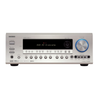
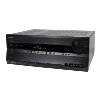
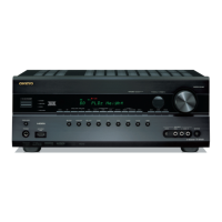
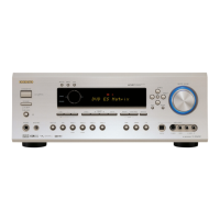
Lists Black, Golden, and Silver models.
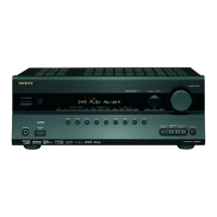
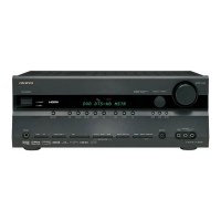
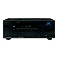
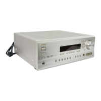
Lists Black and Silver models.
Lists the Golden model variant.
Critical components for fire/shock risk, replacement instructions.
Details on power, THD, impedance, video inputs/outputs, and frequency response.
FM/AM specs, power supply, dimensions, weight, and other general details.
Procedures for replacing fuses and initializing the unit to factory settings.
How to check the microprocessor version and details on the memory backup system.
Visual representation of component placement on the first part of the exploded view.
Visual representation of component placement on the second part of the exploded view.
Illustrates the signal paths for audio inputs, tuner, digital sources, and outputs.
Detailed circuit diagram for the audio input stage, showing component connections.
Circuit diagram detailing the Digital Signal Processing (DSP) section and its connections.
Circuit diagram for the first part of the power amplifier section, showing transistor and resistor details.
Circuit diagram for the second part of the power amplifier section, detailing output stages.
Circuit diagrams for speaker terminal connections, including front, surround, and zone speakers.
Circuit diagrams for the power supply units, detailing AC input and voltage selection.
Circuit diagram for the front panel display and related controls.
Detailed circuit diagram for video inputs, outputs, and processing.
Diagram showing how various PC boards are interconnected.
Component layout view of the Video PC Board (Side A).
Component layout view of the Video PC Board (Side B).
Component layout view of the Display PC Board (Side A).
Component layout view of the Display PC Board (Side B).
Component layout view of the DSP PC Board (Side A).
Component layout view of the DSP PC Board (Side B).
Component layout view of the Switch PC Board (Side A).
Component layout view of the Headphone Jack PC Board (Side A).
Component layout view of the Front Optical/IR PC Board (Side A).
Component layout view of the IR Terminal PC Board (Side A).
Component layout view of the Amplifier PC Board (Component Side).
Component layout view of the Secondary Terminal-2 PC Board (Component Side).
Component layout view of the SBR Amplifier PC Board (Component Side).
Component layout view of the Thermal Sensor PC Board (Component Side).
Component layout view of the Power Supply-1 PC Board (Component Side).
Component layout view of the Power Supply-2 PC Board (Component Side).
Component layout view of the Secondary Terminal-1 PC Board (Component Side).
Component layout view of the Speaker Terminal PC Board (Component Side).
Component layout view of the Center Speaker Terminal PC Board (Component Side).
Component layout view of the Driver Amplifier PC Board (Component Side).
Detailed description of microprocessor Q701 pins 1 through 50, including I/O and function.
Detailed description of microprocessor Q701 pins 51 through 100, including I/O and function.
Steps for adjusting idling current after transistor or board replacement, including test points.
Diagram illustrating test points and trimming resistors for idling current adjustment on amplifier boards.
| Channels | 7.1 |
|---|---|
| Total Harmonic Distortion | 0.08% |
| Frequency Response | 10 Hz - 100 kHz |
| HDMI Inputs | 2 |
| HDMI Outputs | 1 |
| Component Video Inputs | 3 |
| Component Video Outputs | 1 |
| Digital Audio Inputs (Optical) | 2 |
| Digital Audio Inputs (Coaxial) | 2 |
| Audio Formats Supported | Dolby Digital, DTS, Dolby Pro Logic II |
| THX Certified | No |
| Input Sensitivity/Impedance | 200 mV/47 kΩ |
| Signal-to-Noise Ratio | 100 dB |
| Power Output (per channel) | 90 Watts @ 8 Ohms |
| Video Inputs/Outputs | Composite: 4 Inputs / 1 Output, S-Video: 1 Output |