- 17 -
Chassis Service Adjustment Procedures
All service adjustments are factory preset and should not require adjustment unless controls and/or
associated components are replaced.
Note: Connect the (-) lead of the voltmeter to the appropriate ground. Use IC803’s heat sink when the HOT ground
symbol ( ) is used. Otherwise, use COLD ground ( ) — Tuner shield, IC451’s heat sink or FA2.
MOMENTARILY CONNECT A JUMPER FOR ENTERING SERVICE MODE (FA1 to FA2 )
131.0V B+ Voltage Confirmation
1. Set the Bright and the Picture to Minimum by
using the Picture Menu.
2. Connect the DVM between C809(+ side) and cold
ground ( ).
3. Confirm that B+ voltage is 131.0V ± 2.5V. This
voltage supplies B+ to the Horizontal Output &
Flyback circuits.
Source Voltage Chart
120V AC line input. Set the Bright and the Picture to
Minimum by using the Picture Menu. Use cold ground
(
) for the (-) lead of the DVM.
Adjust Picture Menu for normalized video adjustments.
High Voltage Check
1. Select an active TV channel and confirm that
horizontal is in sync.
2. Adjust Brightness and Picture using Picture Icon
menu so video just disappears.
3. Confirm B+ 131V is within limit.
4. Using a high voltage meter confirm that the High
Voltage at the CRT anode is 29.25kV ± 1.25kV.
DVD Voltage Check
Play a DVD TEST DISC and measure the following:
IC6501
IC001
IC002
IC552
C572
IC101
TP47R
TP47G
TP47B
TUNER
TPE1
TPE11
TPE10
Fuse
TP12
TP88
T501
T551
FBT
C552
C551
TPD8
TPD9
D554
Screen Focus
TPD7
TPD2
T502
Q501
Q551
IC2321
IC2201
Q002
Q801
RL801
T801
L802
Q802
L803
C809
IC451
Q804
D001
IC551
IC803
HOT
GND
COLD
GND
IC2302
1
81
1
13
12
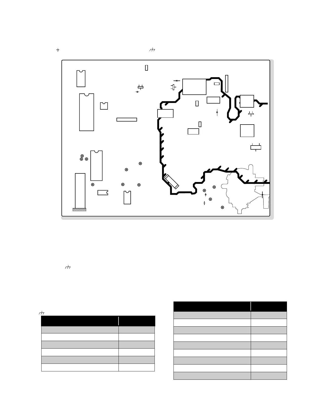
Figure 17. A-Board Main Components and Test Points
LOCATION VOLTAGE
TPD8 27.4V ± 2V
TPD9 13.0V ± 2V
C552 (+) side 8.0V ± 1V
IC551 Pin3 9.0V ± 0.5V
D554 Cathode 220V ± 15V
C572 (+) side 5.0V ± 0.25V
LOCATION VOLTAGE
JJ1 pin1 - P2 pin1 (TPJJ5) -11.0V ± 1V
JJ1 pin3 - P2 pin3 (TPJJ10) 11.0V ± 1V
JJ1 pin5 - P2 pin5 (TPJJ6) 5.0V ± 0.25V
JJ1 pin6 - P2 pin6 (TPJJ7) 5.0V ± 0.25V
W6 pin2 - P1 pin7 (TPW7) 2.5V ± 0.125V
W6 pin4 - P1 pin4 (TPW6) 2.5V ± 0.125V
W6 pin6 - P1 pin6 (TPW5) 5.0V ± 0.25V
W6 pin8 - P1 pin8 (TPW3) 9.0V ± 0.45V
W6 pin10 - P1 pin10 (TPW4) 5.0V ± 0.25V





 To Next Page