Signal Name Function
CH_SEL[0] Synchronous Signal for CODEC (For MOH#1/Page#1)
CH_SEL[1] Synchronous Signal for CODEC (For MOH#2/Page#2)
CH_SEL[2] Synchronous Signal for CODEC (For RMT)
CKE Clock Enable: CKE signal for SDRAM
CKIO Clock I/O For bus clock of SDRAM (IC505, IC506) and ASIC (IC102). CPU (IC200) outputs the clock of four times
frequency as many as Source clock (16.384MHz).
nCS0 Chip Select 0: Chip select signal for flash memory
nCS1 Chip Select 1: Chip select signal for BUS-M Card
nCS2 Chip Select 2: Chip select signal for SDRAM
nCS3 Chip Select 3: Chip select signal for the expanded SDRAM (Future Option, Reserve at present.)
nCS4 Chip Select 4: Chip select signal for SRAM
nCS5 Chip Select 5: Chip select signal for ASIC
nCS6 Chip Select 6: Chip select signal for USB I/F, SD card I/F and SD card I/F
nCS_FLASH Chip Select for Flash memory CS signal for IC503
nCS_SDB Chip Select for SD card I/F
nCS_SRAM0 Chip Select for SRAM0: CS signal for IC621
nCS_SRAM1 Chip Select for SRAM1: CS signal for IC622
nCS_USB Chip Select for USB I/F
nCTS2 Clear To Send from RS-232C connector
CTS_RMT Clear to Send: Flow signal for modem
CT_C8 Clock8.192MHz clock outputted from ASIC (IC102)
CT_D[7:0] CT Data Bus: Two-way serial data bus to which the drive from any card is possible in the system.
CT_FRAME Frame Signal: 8KHz frame signal outputted from ASIC (IC102)
CT_NETREF Backup Synchronous Signal (MAX 2MHz) 8KHz signal output from
C_CS[0] Chip Select For RMT (Reserved)
D[31:0] Data Bus
nDACK0-1 DMA Acknowledge: For USB I/F
DCD Data Carrier Detect
DCLK_RMT Codec Clock (8MHz): For RMT
nDC_ALM DC ALARM:DC alarm signal; Indicates the declined DC voltage. (L: Alarm condition)
DIN_RMT Codec Data Input: For RMT (Reserved)
DOUT_RMT Codec Data Output: For RMT (Reserved)
nWE[0:3] Data Input/Output Mask (Write Enable): DQM signal for SDRAM and WE signal for each memory IC and ASIC
nWE1, nWE2, nWE3
nDREQ0-1 DMA Request: For USB I/F
DSR2 Data Set Ready from RS-232C connector
DSR_RMT Data Set Ready from RS-232C connector
DTR2 Data Terminal Ready to RS-232C connector
EC_AD[15:0] Address of EC Synchronous Bus, Data Bus (4MHz)
EC_nCBE[1:0] EC Bus Command/Byte Enable: The initiator drives as bus command in the address phase and as byte enable in the
data phase.
EC_nCDET EC Line Card Detection Signal Asynchronous interrupting signal
EC_CLK Clock of EC Synchronous Bus (8MHz) All the EC bus signal except nRESET/EC_INT operates in sync with this
signal.
EC_nFRAME EC Cycle Frame Signal: This indicates the drive by initiator and the execution of ECI bus cycle.
EC_nINT EC Interrupting Signal: This is asserted, when slave interrupt occurs.
EC_PAR Parity Bit of EC Synchronous Bus: Drive by applying even parity to AD[15:0] and CBE[1:0]. (4MHz)
EC_nPERR EC Parity Error: Flag indicating error status by parity flag
EC_nRST EC Reset Input: System reset input signal
EC_nSTOP EC Bus Stop Signal: This is asserted, when target requests transaction halt to initiator.
EC_nTRDY EC Target Ready Signal: This indicates the drive by target and the possible data transfer.
nFAN_ALM Fan Alarm: It goes Low at the error of the L Power Supply’s FAN. It goes High when the FAN is normal and, Power
Supply M, which does not carry the FAN, are used.
HALT This alarms the occurrence of the declined DC voltage to line card. H: Active L: Normal
nINIT System Initialization Switch Input: L: At system initialization, H: At normal start-up
nIRQ_ASIC Interrupt Request from ASIC: This indicates ASIC requests interrupt.
nIRQ_SDB Interrupt Request from SD card I/F: This indicates SD card I/F requests interrupt.
nIRQ_BUSM Interrupt Request from BUS-M card I/F: This indicates BUS-M card I/F requests interrupt.
nIRQ_USB Interrupt Request from USB I/F: This indicates USB I/F requests interrupt.
LA[22:1] Address bus
nLB Lower Byte Select: This indicates Lower byte select signal of SRAM
LD[15:0] Data Bus
LDHW[1:0] Down Highway: Data output terminal connected to codec etc. as down data signal of local highway
nLEDALM Alarm display L: On
nLEDRUN RUN display L: On
nLOS Loss of synchronous signal: Reserve at present
LHWCLK[0] Highway Clock Signal (8MHz): Bit clock of local highway.
LUHW[1:0] Up Highway: Data input terminal connected to codec etc. as up data signal of local highway.
33
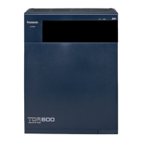
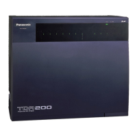
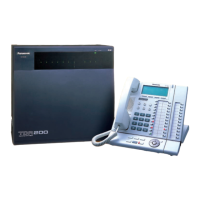
KX-TDA600BX
 Loading...