S-1
S1. About Indication of The Schematic Diagrams .......................... S-1
S1.1. Important Safety Notice......................................................... S-1
S2. Voltage Chart ........................................................................... S-2
S2.1. Monitor P.C.B . ...................................................................... S-2
S2.2. EVF P.C.B. ........................................................................... S-2
S2.3. Mic Jack P.C.B. .................................................................... S-2
S2.4. Front P.C.B. .......................................................................... S-2
S3. Block Diagram .......................................................................... S-3
S3.1. Overall Block Diagram .......................................................... S-3
S4. Schematic Diagram .................................................................. S-4
S4.1. Interconnection Diagram ....................................................... S-4
S4.2. EVR INT 1 Schematic Diagram ............................................. S-8
S4.3. EVR INT 2 Schematic Diagram ............................................. S-8
S4.4. Battery INT Schematic Diagram ............................................ S-9
S4.5. AV Jack Schematic Diagram ............................................... S-10
S4.6. Side R Schematic Diagram ................................................. S-11
S4.7. Side R Operation Schematic Diagram ................................ S-12
S4.8. Monitor Schematic Diagram ................................................ S-13
S4.9. EVF INT Schematic Diagram .............................................. S-14
S4.10. EVF B/L Schematic Diagram ............................................ S-14
S4.11. Handle Zoom Schematic Diagram ................................... S-15
S4.12. Mic Jack Schematic Diagram ............................................ S-15
S4.13. Zoom Schematic Diagram................................................. S-16
S4.14. Front Schematic Diagram ................................................. S-16
S4.15. S/S Power Schematic Diagram ......................................... S-17
S4.16. LCD Det Schematic Diagram ............................................ S-17
S4.17. Eject Schematic Diagram .................................................. S-17
S4.18. CCD Flex Schematic Diagram .......................................... S-18
S4.19. Holl Sensor Flex Schematic Diagram ............................... S-22
S5. Print Circuit Board .................................................................. S-23
S5.1. EVR INT 1 P.C.B. ............................................................... S-23
S5.2. EVR INT2 P.C.B. ................................................................ S-23
S5.3 Battery INT P.C.B. ............................................................... S-24
S5.4. AV Jack P.C.B . ................................................................... S-25
S5.5 Side R P.C.B. ...................................................................... S-26
S5.6 Side R Operation P.C.B. ...................................................... S-27
S5.7. Monitor P.C.B. ..................................................................... S-28
S5.8. EVF INT P.C.B. .................................................................. S-29
S5.9. EVF P.C.B. ......................................................................... S-29
S5.10. Handle Zoom P.C.B. ......................................................... S-30
S5.11. Mic Jack P.C.B. ................................................................. S-30
S5.12. Zoom P.C.B. ..................................................................... S-31
S5.13. Front P.C.B. ...................................................................... S-31
S5.14. S/S Power P.C.B. .............................................................. S-32
S5.15. LCD Det P.C.B. ................................................................. S-32
S5.16. Eject P.C.B. ...................................................................... S-33
S5.17. CCD Flex .......................................................................... S-34
S5.17.1. CCD Flex (Component Side) ......................................... S-34
S5.17.2. CCD Flex (Foil Side) ...................................................... S-35
S5.18. Holl Sensor Flex ................................................................ S-36
S6. Replacement Parts List ......................................................... S-37
S7. Exploded Views ...................................................................... S-44
S7.1. Frame and Casing Section(1) ............................................. S-44
S7.2. Frame and Casing Section(2) ............................................. S-45
S7.3. Camera Lens Section......................................................... S-46
S7.4. LCD Section ........................................................................ S-47
S7.5. Video Mechanism Section ................................................... S-48
S7.6. Packing Parts and Accessories Section .............................. S-49
Table of contents
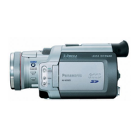
Service Manual
Digital Video Camera
Vol. 1
NV-MD10000GC
NV-MD10000GK
VM0509039CE
Diagrams and Replacement
Parts List
1.Although reference number of the parts is indicated on the P.C.B. drawing and/or
schematic diagrams, it is NOT mounted on the P.C.B. when it is displayed with "$" mark.
2.It is only the "Test Round" and no terminal (Pin) is available on the P.C.B.
when the TP (Test Point) indicated as "٨" mark.
3.The voltage being indicated on the schematic diagram is measured in
"Standard-Playback" mode when there is no specify mode is mentioned.
4.Although the voltage and waveform available on here is measured with standard frame,
it may be differ from actual measurement due to modification of circuit and so on.
5.The voltage being indicated here may be include observational-error (deviation) due to
internal-resistance and/or reactance of equipment. Therefore, handle the value
indicated on here as reference.
6.Use the parts number indicated on the Replacement Parts List .
COMPONENTS IDENTIFIED WITH THE MARK HAVE THE SPECIAL CHARACTERISTICS
FOR SAFETY. WHEN REPLACING ANY OF THESE COMPONENTS USE ONLY THE S AME TYPE.
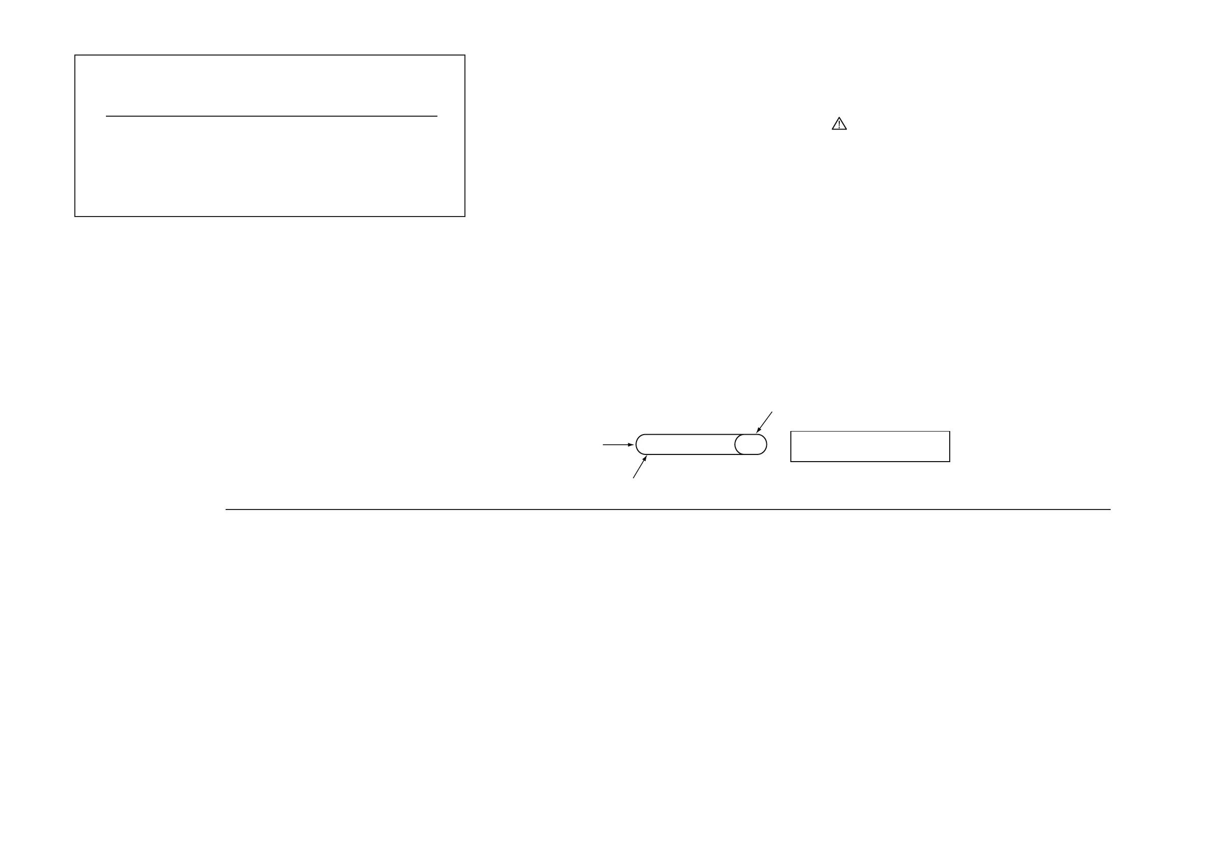
7.Indication on Schematic diagrams:˴
OFTR
FEP
Circuit name being connected.
Name of Signal
This signal is connected
to the EFP schematic diagram