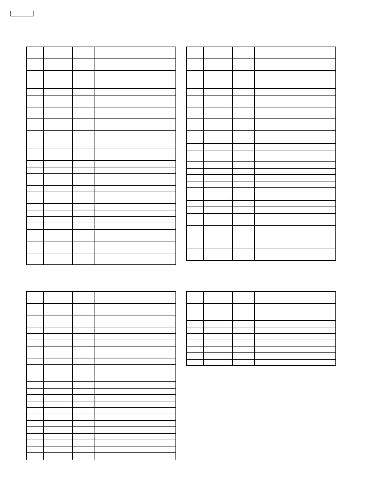
Pin
No.
Mark I/O Function
1 CENVD — D signal det. capacitor connection
terminal
2 LDO O Laser amp output terminal
3 APCPD I Photo diode light quantity det. input
terminal
4 LD IN I Laser amp reverse input terminal
5 APC REF I APC amp criterion voltage input
terminal
6 TEMP IN I Temperature sensor amp input
terminal
7 TEMP O Temperature sensor amp output
terminal
8 ADIP O ADIP signal output terminal
9 TOFS I Tracking error offset adjustment
terminal
10 TBAL I Tracking ballance adjustment
terminal
11 TE O Tracking error signal output terminal
12 CRS IN I Track cross input terminal
13 TGAIN I Tracking gain adjustment input
terminal
14 LNP O Lens position signal output terminal
15 AB GAIN I APP compensation signal gain
adjustment terminal
16 FE O Focus error signal output terminal
17 AS GAIN I AS gain adjustment terminal
18 FBAL I Focus ballance adjustment terminal
19 AS/MON3T O AS/3TMON signal output terminal
20 CEA I 3T envelope det. capacitor
connection terminal
21 BDO/TRCR
S
O BDO/Track cross signal output
terminal
22 CBD O O BDO detection capacitor connection
terminal
Pin
No.
Mark I/O Function
1 REG B — 3.3V external transistor control
terminal (Not used, open)
2 REG M — 3.3V regular output monitor terminal
(Not used, connected to GND)
3 NC — Not used, open
4 OPO O Op-amp output terminal
5 OP- O Op-amp invert output terminal
6 OP+ O Op-amp non-invert output terminal
(Not used, connected to GND)
7 Vcc I Power supply terminal
8 1/2 PVcc2 O 1/2 PVcc output terminal 1
(Connected to GND through
capacitor)
9 PVcc2 I Power supply terminal for driver
10 PGND2 — GND terminal
11 VO4- O Tracking coil driver output terminal
12 VO4+ O Tracking coil driver output terminal
13 VO3- O Focus coil driver output terminal
14 VO3+ O Focus coil driver output terminal
15 VO2- O Traverse motor drive output terminal
16 VO2+ O Traverse motor drive output terminal
17 VO1- O Spindle motor drive output terminal
18 VO+ O Spindle motor drive output terminal
19 PGND — GND terminal
20 PVcc1 I Power supply terminal
Pin
No.
Mark I/O Function
23 OFT O O Off track detection signal output
terminal
24 GND — GND terminal
25 OFT IN I Off track detection signal input
terminal
26 VCC I Power supply terminal (+3V)
27 NRFDET/
OFTR
O NRFDET/off track signal output
terminal
28 NRFLD I Serial command latch signal input
terminal
29 RF DATA I Serial command data signal input
terminal
30 RFCK I Serial command clock input terminal
31 NRFSTBY I Standby control signal input terminal
32 OUT RF O EFM signal output terminal
33 CRF AGC — RFAGC capacitor connection
terminal
34 EQ IN I EQ input terminal
35 ARFO O RF amp. output terminal
36 SVREF I Reference voltage input terminal
37 VREF O Reference voltage output terminal
38 RF1 I RF1 signal input terminal
39 RF2 I RF2 signal input terminal
40 F1 I F1 signal input terminal
41 F2 I F2 signal input terminal
42 CLPF1 — APP compensation LPF capacitor
connection terminal
43 CLPF2 — RF equalizer adjustment resistor
connection terminal
44
~47
A
~D
I Beam A~D signal input terminal
48 CENVC — Beam E signal detection capacitor
connection terminal
Pin
No.
Mark I/O Function
21 1/2 PVcc1 O 1/2 PVcc output terminal 1
(Connected to GND through
capacitor)
22 VREF I Reference voltage input
23 IN1 I Spindle motor drive input terminal
24 PC1 I Power cut 1 input terminal
25 IN2 I Traverse motor drive input terminal
26 PC2 I Power cut 2 input terminal
27 IN3 I Focus drive input terminal
28 IN4 I Tracking drive input terminal
12 Terminal Function of IC´s
12.1. IC1 (AN8772FHQ) : RF AMP
12.2. IC2 (AN8814SB-E1) : FOCUS/TRACKING COIL, SPINDLE/TRAVERSE
MOTOR DRIVE
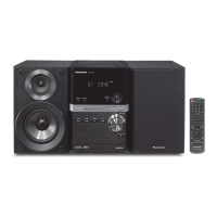
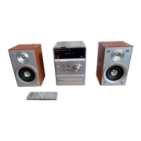
26
SA-PM30MD