Do you have a question about the Philips MRV640 and is the answer not in the manual?
Details specifications for analogue inputs and outputs, including External 1 and 2.
Provides critical safety guidelines for servicing and handling the unit.
Highlights important warnings, including ESD and laser hazards.
Provides steps for disassembling and assembling the unit.
Explains the diagnosis interface for checking hardware faults.
Details interfaces for controlling the player, including Trade and Virgin modes.
Provides an overview of nuclei, numbers, and error codes for the Digital Board.
Presents a high-level block diagram of the digital board's architecture.
Shows the control block diagram for the analog and UP sub boards.
Illustrates the interconnections between major boards and components.
Provides a layout of test points on the analog board with associated waveforms.
Shows the location of test points on the UP Sub Board.
Details the locations of test points on the digital board.
Circuit diagram for the digital board's 1394 interface.
Circuit diagram for the digital board's Video Input Processors (VIPs).
Circuit diagram and PWB layout for the analog board's power supply unit.
Circuit diagram and PWB layout for the UP Sub Board's central controller.
Circuit diagram for the digital board's IDE, UARTs, RESET, and BE interfaces.
Circuit diagram for the digital board's video input/output.
Details the procedure for reprogramming the NVM on the microprocessor sub PCB.
Outlines the procedure for upgrading sets with a unique number after repair.
Describes aligning sets after replacing the Boot EEPROM with Digital Board Chrysalis.
Overview of the 2nd generation digital board based on the Chrysalis IC.
Details the interfaces between Chrysalis and the Basic Engine module.
Explains the reset concept and signals for the Chrysalis board.
Details the service UART interface for diagnostics and software updates.
Describes the TEA1507 IC for power supply control.
Describes the ADV7196A IC for progressive scan video encoding.
Explains the functional principle of the flyback converter power supply.
Describes the tuner, IF amplifier, video demodulator, and sound processor components.
Explains how video and audio signals are handled for recording.
Describes the power supply enablement and the 1.8V core voltage generation.
Overview of the analog board's components and their functionality.
Explains analog-to-digital and digital-to-analog audio conversion using UDA1361TS and UDA1334BTS.
Describes how video and audio signals are processed during playback.
Describes the integration of progressive scan video output generation.
Provides a block diagram and pin descriptions for the TMP87CH74AF microcontroller.
Describes the STV6618 IC used as an analog board video switch matrix.
| DVD Recording Format | DVD+R, DVD+RW, DVD-R, DVD-RW |
|---|---|
| Recording Format | MPEG2 |
| TV Tuner | Yes |
| Progressive Scan | Yes |
| Remote Control | Yes |
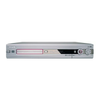
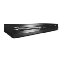
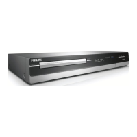
| Type | DVD Recorder |
| Disc Types | CD, DVD |
| Playback Format | JPEG, MP3 |
| Audio System | Dolby Digital |
| Connections | Component video output, Composite video output, S-Video output, Coaxial Digital Audio, Optical Digital Audio |
| Connectors | Component Video Out, S-Video Out, Composite Video Out, Coaxial Digital Audio Out, Optical Digital Audio Out, RF In/Out |