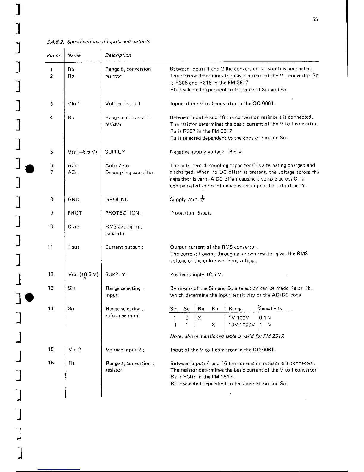
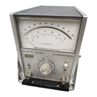
3.4.6.2.
Specifications
of inputs and outputs
I
I
I
l
l
l
l
l
l
l
l
l
l
l
l
I
2
8
I
10
11
55
Vss
(-8,5
V)
AZc
^Zc
Description
Range b, conversion
resrstor
Voltage input I
Range a, conversion
resistor
SUPPLY
Auto Zero
Dccoupling capacitor
3
5
6
7
Between inputs 1 and 2 the conversion
resistor b is connected.
The resistor determines
the basic current of the
V'l
convertor
Rb
is R308
and
R316
in
the
Pl\4
2517
Rb is selected dependent
to the code
of Sin and
So.
Inpur ol the
V
to
I
convertor
rn
the OO 0061.
Between
input 4
and
16 the conversion
resistor a is connected.
The resistor determines the basic current
of the
V
to
I
convertor.
Ra is R307 in the
PlVl
2517
Ra
is selected
dependent to the code of Sin
and So.
Negative
supply
voltage
-8.5
V
The auto zero decoupling capacitor
C
is
alternatrng charged
and
discharged.
When
no
DC offset
is
present,
the voltage across the
capacitor
is zero. A DC offset causing a
voltage across C,
is
compensated
so no influence is seen upon the
output signal.
Supply
zero.
ü
Protection input.
Output current of the
Rlvls
convertor.
The current
flowing
through a
known resistor
gives
the
RIVIS
voltage of the unknown
inpLrt voltage.
Positive
supptv
8,5
V.
By means of the Sin and So a selection can be
made Ra or Rb,
which determine the ioput sensitivity of the
AD/DC conv.
Note:
above
mentioned
table
is valid for
PM
2517.
Input of the
V
to
I
convertor
in the OO 0061.
Between
inputs 4
and
l6
the
conversion resistor
a is connected.
The resistor determines the basic current of the
V
to
I
convertor
Ra is
R307
in the
Plvl 2517.
Ra is selected dependent to the code of Sin and So.
GND
PROT
Crms
I our
vdd
(+.8,5
v)
Sin
Vin 2
Ra
GROUND
PROTECTION
R lvlS
äveraging
capacitor
Current output
SUPP
LY
;
Range
selecting
input
Range
selecting
reference input
Voltage input 2
;
Range
a, conversion
resistor
l.
l
I
I
.l
I
.l
l
l
l5
Sin So
I
Ra Rb
I
Range
1V.'r00v
10.1
v
10v,1000v
lr
v