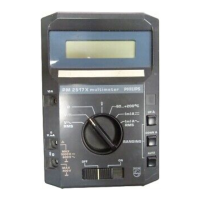
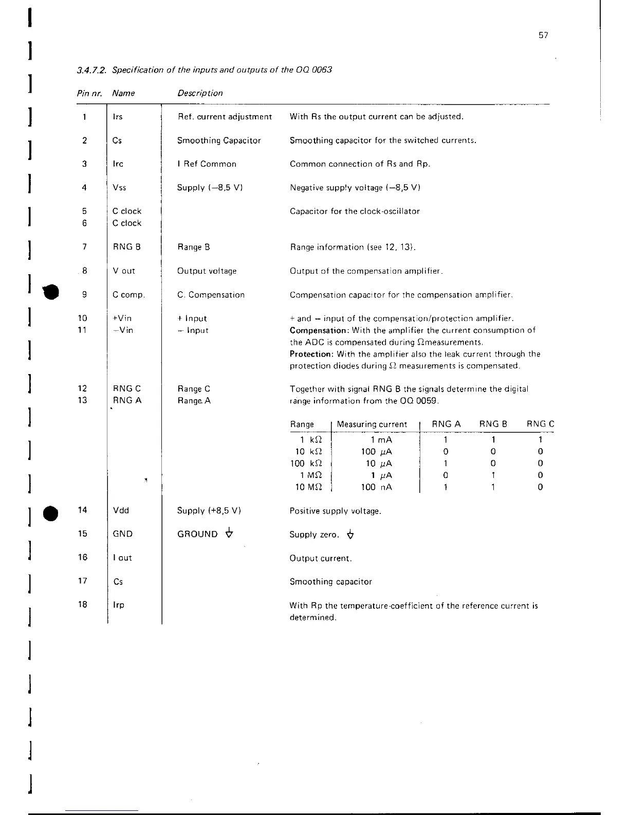
3.4.7.2.
Specification of the
inputs and
outputs
of the OA 0063
Pin
nr. Name Desciption
Ref . current adjustment
Smooth ing Capacitor
I ReI
Common
Supply
(-8,5
V)
Range
B
Output voltage
C. Compensation
+
Input
-
Input
Range
C
Range. A
Su
pply
(+8,5
V)
GROUND
+
57
RNG A RNG B
RNG
C
1
0
1
0
I
I
0
0
1
1
1
0
0
0
0
1
2
3
5
6
7
8
9
10
l1
lrs
trc
C clock
C clock
RNG
B
v
out
C comp.
With Rs the output current can be adjusted.
Smoothing capacitor
for the switched currents.
Common connection of
Rs
and
Rp.
Negative supply voltage
{-8,5
V)
Capacitor
for
the clock-oscillator
Range information
(see
12, 13).
Output of the compensation ampiifrer.
Compensation capacrtor
for
the compensation amplifier.
+
and
-
input
of the compensation/protection
amplifier.
Compensation:
With
the amplifier the current consumption
of
the
ADC is compensated during Omeasurements.
Protection: With the
amplifier also the
leak current through the
protection
diodes
during O measurements is
compensated.
Together
with
signal RNG B the signals determine the
digital
range information from
the OO 0059.
Range
lvleasuring
current
12 RNG
C
RNG A
1ko
10
ko
100
ko
1l\,10
1O MQ
lmA
100
/rA
10
irA
lgA
100 nA
't4
tc
to
17
18
vdd
GND
I
out
trp
Positive
supply
voltage.
Supply zero.
$
OutPut current.
Smooth
ing
capacitor
With
Rp
the temperature'coefficient of the reference current is
determined.