TDA8950_2 © NXP B.V. 2009. All rights reserved.
Product data sheet Rev. 02 — 11 June 2009 12 of 39
NXP Semiconductors
TDA8950
2 × 150 W class-D power amplifier
9. Limiting values
[1] V
P
is the supply voltage on pins VDDP1, VDDP2 and VDDA.
10. Thermal characteristics
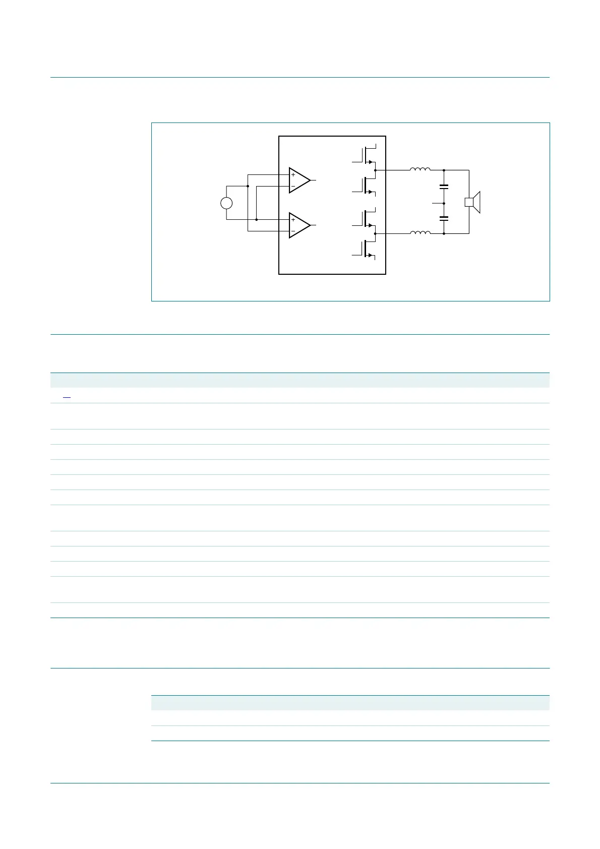
Fig 7. Input configuration for mono BTL application
V
in
IN1P
OUT1
power stage
mbl466
OUT2
SGND
IN1M
IN2P
IN2M
Table 6. Limiting values
In accordance with the Absolute Maximum Rating System (IEC 60134).
Symbol Parameter Conditions Min Max Unit
V
P
[1]
supply voltage Standby, Mute modes; V
DD
− V
SS
-90 V
I
ORM
repetitive peak output current maximum output current limiting 9.2 - A
T
stg
storage temperature −55 +150 °C
T
amb
ambient temperature −40 +85 °C
T
j
junction temperature - 150 °C
V
MODE
voltage on pin MODE referenced to SGND 0 6 V
V
OSC
voltage on pin OSC 0 SGND + 6 V
V
I
input voltage referenced to SGND; pin IN1P; IN1M;
IN2P and IN2M
−5+5 V
V
PROT
voltage on pin PROT referenced to voltage on pin VSSD 0 12 V
V
ESD
electrostatic discharge voltage Human Body Model (HBM) −2000 +2000 V
Charged Device Model (CDM) −500 +500 V
I
q(tot)
total quiescent current Operating mode; no load; no filter; no
RC-snubber network connected
-75 mA
V
PWM(p-p)
peak-to-peak PWM voltage on pins OUT1 and OUT2 - 120 V
Table 7. Thermal characteristics
Symbol Parameter Conditions Typ Unit
R
th(j-a)
thermal resistance from junction to ambient in free air 40 K/W
R
th(j-c)
thermal resistance from junction to case 1.1 K/W