TDA8950_2 © NXP B.V. 2009. All rights reserved.
Product data sheet Rev. 02 — 11 June 2009 13 of 39
NXP Semiconductors
TDA8950
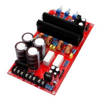
2 × 150 W class-D power amplifier
11. Static characteristics
[1] V
P
is the supply voltage on pins VDDP1, VDDP2 and VDDA.
[2] The circuit is DC adjusted at V
P
= ±12.5 V to ±42.5 V.
[3] Unbalance protection activated when V
DDA
> 2 ×|V
SSA
| OR |V
SSA
| > 2 × V
DDA
.
[4] With respect to SGND (0 V).
[5] The transition between Standby and Mute modes has hysteresis, while the slope of the transition between Mute and Operating modes is
determined by the time-constant of the RC network on pin MODE; see Figure 8.
[6] DC output offset voltage is gradually applied to the output during the transition between Mute and Operating modes. The slope caused
by any DC output offset is determined by the time-constant of the RC network on pin MODE.
[7] At a junction temperature of approximately T
act(th_fold)
− 5 °C, gain reduction commences and at a junction temperature of approximately
T
act(th_prot)
, the amplifier switches off.
Table 8. Static characteristics
V
P
=
±
35 V; f
osc
= 345 kHz; T
amb
= 25
°
C; unless otherwise specified.
Symbol Parameter Conditions Min Typ Max Unit
Supply
V
P
[1]
supply voltage Operating mode
[2]
±12.5 ±30 ±40 V
V
P(ovp)
overvoltage protection supply voltage Standby, Mute modes;
V
DD
− V
SS
85 - 90 V
V
P(uvp)
undervoltage protection supply voltage V
DD
− V
SS
20 - 25 V
V
P(ubp)
unbalance protection supply voltage
[3]
-33-%
I
q(tot)
total quiescent current Operating mode; no load; no
filter; no RC-snubber network
connected
- 5075mA
I
stb
standby current measured at 30 V - 480 650 µA
Mode select input; pin MODE
V
MODE
voltage on pin MODE referenced to SGND
[4]
0- 6V
Standby mode
[4][5]
0 - 0.8 V
Mute mode
[4][5]
2.2 - 3.0 V
Operating mode
[4][5]
4.2 - 6 V
I
I
input current V
I
= 5.5 V - 110 150 µA
Audio inputs; pins IN1M, IN1P, IN2P and IN2M
V
I
input voltage DC input
[4]
-0-V
Amplifier outputs; pins OUT1 and OUT2
V
O(offset)
output offset voltage SE; Mute mode - - ±25 mV
SE; Operating mode
[6]
--±150 mV
BTL; Mute mode - - ±30 mV
BTL; Operating mode
[6]
--±210 mV
Stabilizer output; pin STABI
V
O(STABI)
output voltage on pin STABI Mute and Operating modes;
with respect to VSSD
9.3 9.8 10.3 V
Temperature protection
T
act(th_prot)
thermal protection activation
temperature
- 154 - °C
T
act(th_fold)
thermal foldback activation
temperature
closed loop SE voltage gain
reduced with 6 dB
[7]
- 153 - °C