DRS4 Evaluation Board User’s Manual
Page 19 of 43
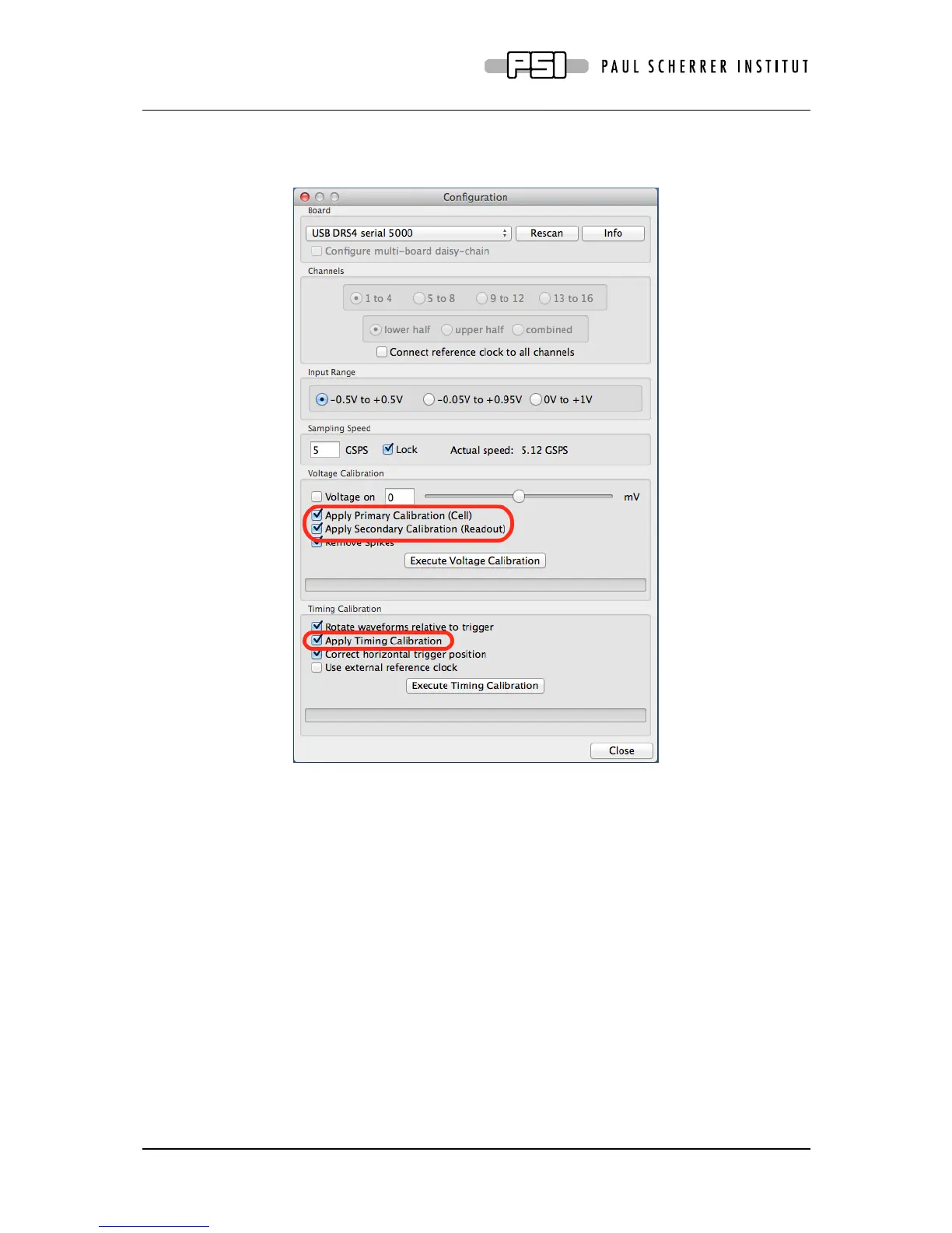
The DRS4 evaluation board is shipped pre-calibrated in amplitude and time. This calibration
can be turned on or off using the check boxes “Display calibrated waveforms” and “Display
timing calibrated waveforms” in the “Config” Dialog:
The calibration can be re-done any time by clicking on the “Execute Voltage Calibration” and
“Execute Timing Calibration” buttons. For the voltage calibration, the inputs are switched to a
calibration voltage generated by a DAC. Three calibration points (-0.4V, 0V, +0.4V) are
measured and an offset and gain is evaluated. For the timing calibration, an internal 100 MHz
clock is sampled in all channels and analyzed to determine the effective width of each cell.
Following picture shows the result of such a timing calibration done at 5 GSPS. The effective
bin width deviates from the nominal value of 0.2 ns by up to ±100 ps, and the integral timing
nonlinearity adds up to almost 0.4 ns, which is typical for the DRS4 chip. Since transistor
parameters have normally gradients over the chip wafer, SCA chips are usually “faster” on
one side than on the other.