DRS4 Evaluation Board User’s Manual
Page 28 of 43
power supply AV
DD
powers only the domino circuit of the DRS4 chip and directly influences
the jitter of the sampling frequency. Long term variations in this power supply (seconds…)
are regulated by the on-chip PLL, but high frequency noise in the MHz region leads directly
to an increase of the PLL jitter. Therefore the evaluation board contains two separate 2.5V
linear regulators for the DRS4 chip, one for the AV
DD
power and one for the DV
DD
power.
Although the DV
DD
power is called “digital power”, it powers also the analog output buffers
of the DRS4 chip and needs the same good quality than the AV
DD
power in order to minimize
the noise of the board.
The DRS4 chip also contains two grounds AGND and DGND. They can be either routed
separately on the board and be connected at the power source, or they can be directly
connected to an overall dedicated ground plane of the PCB. Tests have been shown that the
latter choice gives slightly less noise.
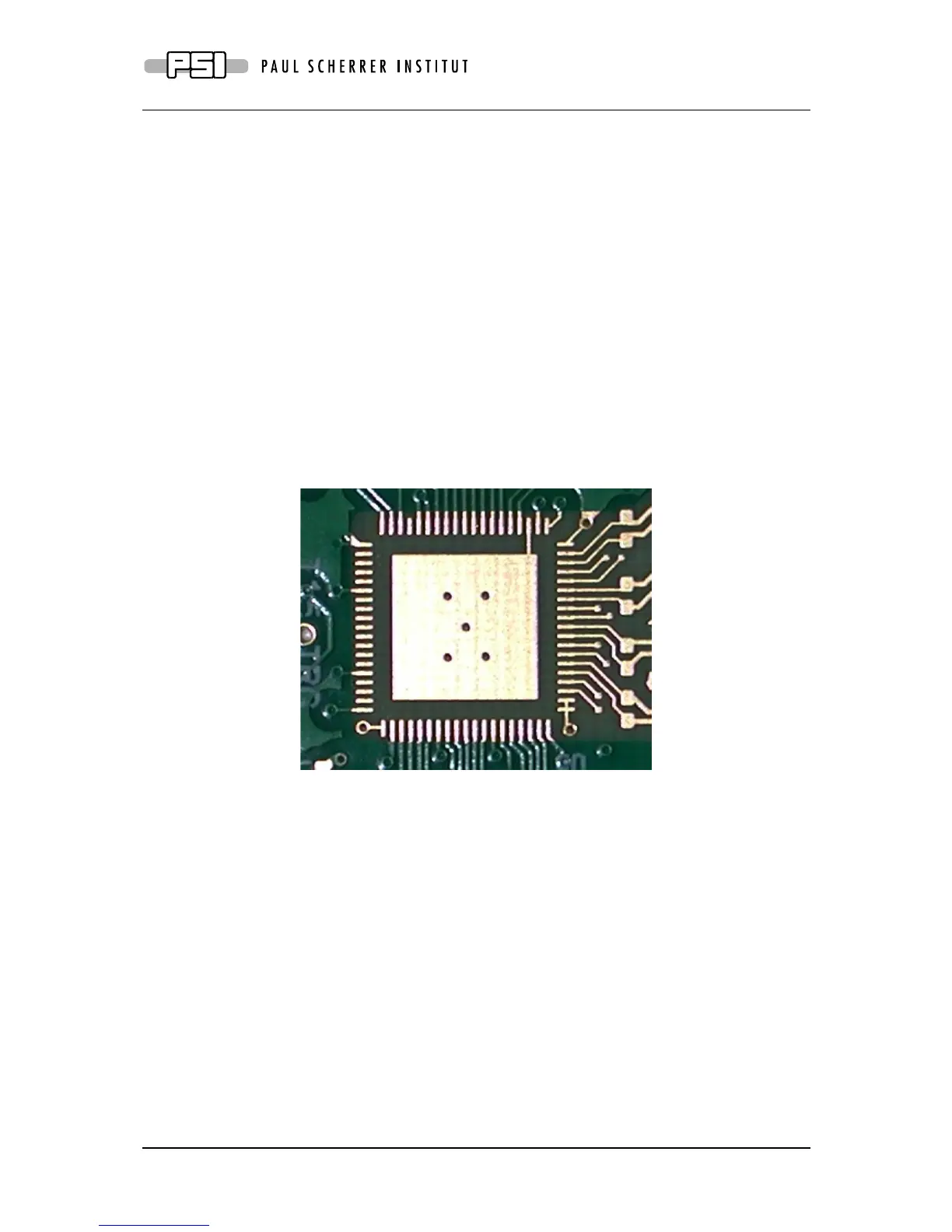
The bottom of the QFN76 package of the DRS4 has an exposed paddle connected to the
internal DGND. It is recommended that this paddle is matched by a PCB pad of similar size
connected to analog ground to achieve the best electrical and thermal performance of the
DRS4. The copper plane should have several vias to achieve a good heat dissipation to flow
through the PCB as shown in Figure 3:
Figure 3: PCB pad under the DRS4 chip
These vias should be solder-filled or plugged. The maximum power dissipation of the DRS4
chip is not critical (350 mW), but an improved thermal stability helps the performance of any
analog chip. To maximize the coverage and adhesion between the DRS4 and the PCB, the
copper plane could be partitioned into several uniform sections, providing several tie points
during the reflow process.
4.2. Analog Input
If non-differential signals should be digitized with the DRS4 chip, they must be converted
into differential signals for the DRS4 inputs. The simplest solution is to connect the IN- inputs
to AGND and to connect the signals directly to the IN+ inputs. This method has however the
disadvantage that the crosstalk and noise immunity of the DRS4 chip are worsened. The
evaluation board V3 uses differential drivers THS4508 from Texas Instruments
®
for this
purpose. These drivers were carefully selected since they have to drive the relatively high
DRS4 input current of almost 1 mA and capacitive load without compromising the analog
bandwidth. The current design gives about 700 MHz (-3 dB) with moderate power
consumption, so that the evaluation board can still be powered from the USB power (500 mA