DRS4 Evaluation Board User’s Manual
Page 4 of 43
1. Introduction
The DRS4 chip, which has been designed at the Paul Scherrer Institute, Switzerland by Stefan
Ritt and Roberto Dinapoli is a Switched Capacitor Array (SCA) capable of digitizing eight
channels at sampling speeds up to 5 GSPS and 1024 sampling points. This chip is available
through the PSI technology transfer program for other institutes and organizations. In order to
simplify the design process to integrate the DRS4 chip into custom electronics, an evaluation
board has been designed, which demonstrates the basic operation of the chip. It has SMA
connectors for four input channels CH1 to CH4, an USB 2.0 connector and MMCX
connectors for triggering and clock synchronization (Figure 1). The board is powered through
the USB port and contains an on-board trigger logic. It comes with MS Windows
®
, Linux and
Mac OSX drivers and two application programs. It is basically equivalent to a four channel 5
GSPS digital oscilloscope.
This manual describes the software installation, the usage of the application programs, and
gives hints for developers seeking to build new electronics around the DRS4 chip.
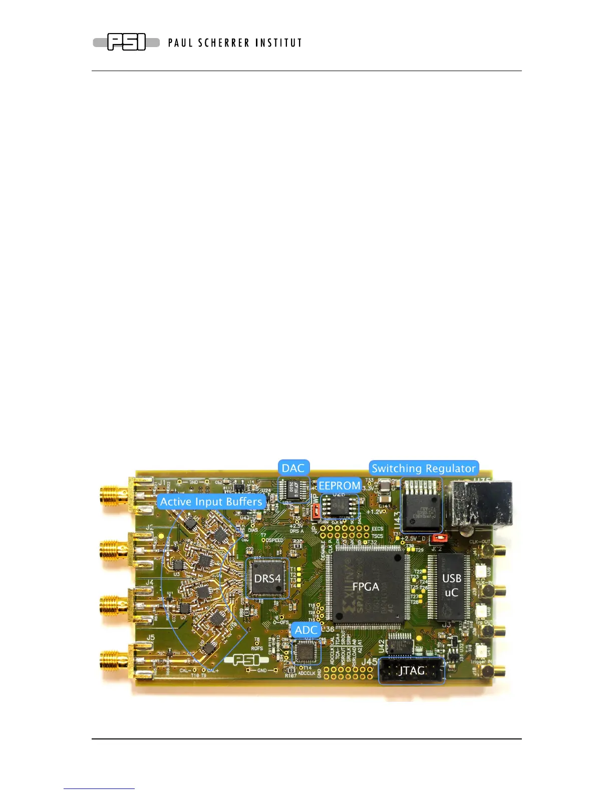
1.1. Board description
Since the DRS4 chip has differential inputs, the board uses four active buffers (THS4508
from Texas Instruments
®
) to convert the 50-Ohm terminated single ended inputs into
differential signals. Analog switches in front of the buffers (ADG901 form Analog Devices
®
)
are used to de-couple the inputs during calibration. Two reference voltages are generated by
the on-board 16-bit DAC to measure the offset and gain of all DRS4 storage cells for
calibration. The four analog inputs are AC coupled and have a input range of 1 V peak-to-
peak. The DRS4 is read out with a 14-bit ADC (AD9245 from Analog Devices
®
) and a FPGA
(Xilinx
®
Spartan 3). The USB connection is implemented with a micro controller (Cypress
®
CY2C68013A). The high speed modus of the USB 2.0 bus allows for data transfer rates of
more than 20 MB/sec.
Figure 1: Picture of the DRS4 Evaluation Board V5 with different components