DRS4 Evaluation Board User’s Manual
Page 5 of 43
For trigger purposes and inter-board synchronization, four MCX connectors are available,
which can be seen on the right side of Figure 1. The Trigger IN works as an external trigger
much like the one of an oscilloscope. The electrical standard is 5V TTL. Although a 50 Ω
termination is possible, the resistor is not soldered by default. This allows using weaker
sources, which cannot drive 5V into a 50 Ω load. Reflections on this line usually do not
matter, since the first leading edge of the trigger is used. To connect a SMA cable to the
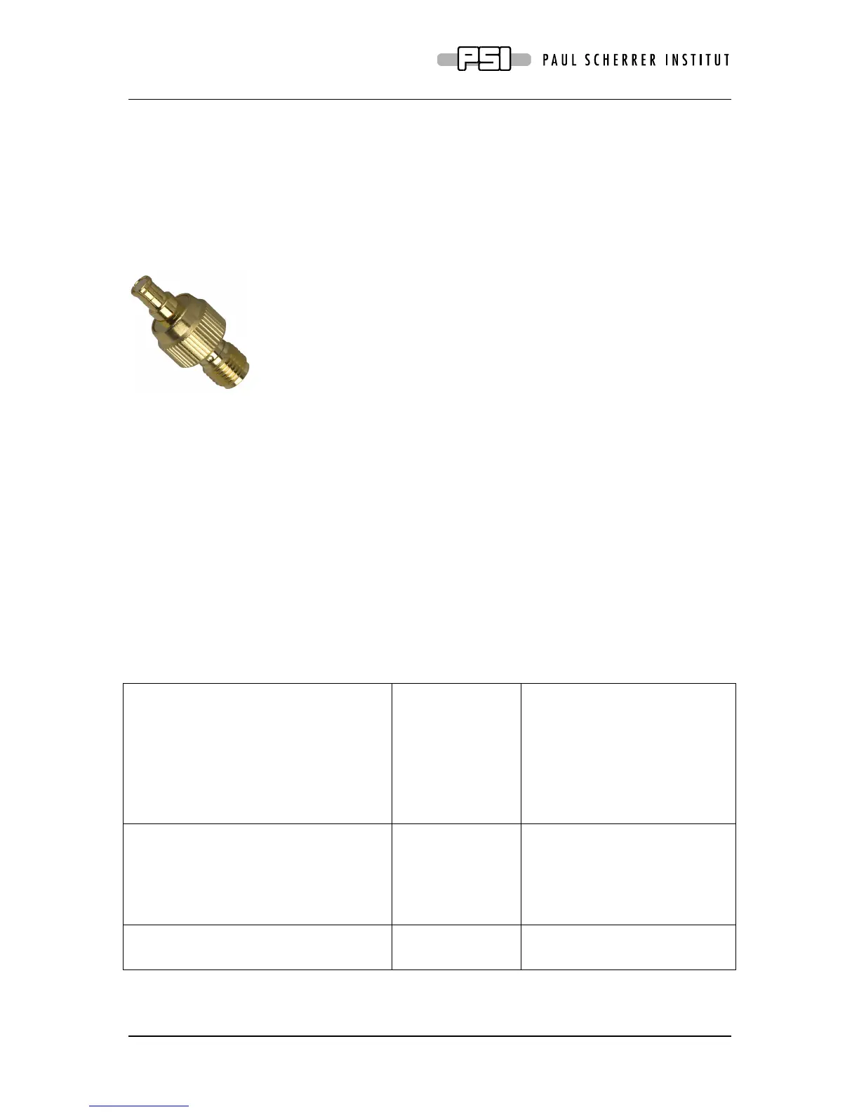
trigger input, a commercial adapter can be used like the one shown in.
Figure 2: MCX-SMA adapter which can be obtained for example form
www.digikey.com (part number ACX1348-ND)
The Trigger OUT signal sends a 150 ns wide pulse when ever the board triggers via the
internal hardware trigger. It does not output a trigger when the board is triggered via software
(for example in the “AUTO” trigger mode of the DRSOsc program). The signal standard is
5V TTL. When terminated with 50 Ω, the signal amplitude will only reach about 2V. As
written above, in most cases the termination should not be necessary.
The Clock IN/OUT signals will be supported in a future firmware version to allow a better
synchronization between different boards for multi-board DAQ systems.
Four on-board discriminators with programmable level allows for self triggering on any of the
four input channels, or a combination of channels supporting coincidences for example. A 1
MBit EEPROM (25LC1025 from Microchip
®
) is used to store the board serial number and
calibration information. Two 14-pin headers carry all important logical signals which allow
easy debugging with a logic analyzer or oscilloscope. A JTAG adapter can be used to update
the FPGA firmware through a Xilinx
®
Platform Cable Adapter.
The specifications of the board inputs is summarized in following table: