EasyManua.ls Logo

PSI DRS4 - Page 8

Default Icon
43 pages
Print Icon
To Next Page IconTo Next Page
To Previous Page IconTo Previous Page
Loading...
DRS4 Evaluation Board User’s Manual
Page 8 of 43
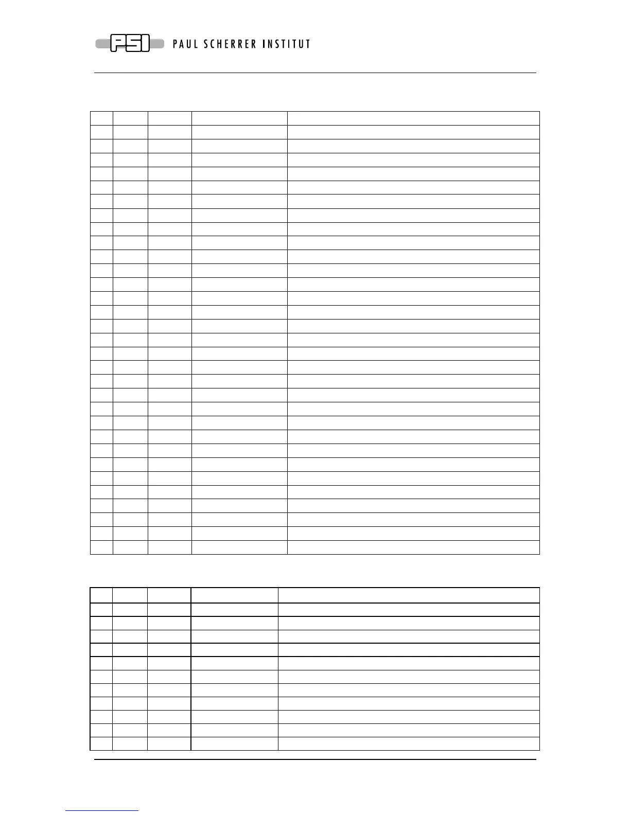
The FPGA firmware implements a set of control and status registers, through which the DRS4
can be controlled and read out. The mapping of the control registers is as follows:
#
Ofs.
Bit
Name
Comment
0
0x00
0
start_trig
Write a "1" to start the domino wave
0
0x00
1
reinit_trig
Write a "1" to stop & reset the DRS chip
0
0x00
2
soft_trig
Write a "1" to stop the DRS chip & read the data to RAM
0
0x00
3
eeprom_write_trig
Write contents of RAM into EEPROM (32kB page)
0
0x00
4
eeprom_read_trig
Read contents of EEPROM into RAM (32kB page)
0
0x02
18
led
1=on, 0=blinks once at beginning of DRS chip readout
0
0x02
19
tcal_en
Switch on (1) / off (0) 100 MHz calib. sig. for DRS chips
0
0x02
21
transp_mode
1=send DRS inputs to outputs ("transparent mode")
0
0x02
22
enable_trigger1
Write a "1" to enable external trigger (LEMO)
0
0x02
23
readout_mode
0:start from first bin, 1:start from domino stop
0
0x02
24
neg_trigger
1=trigger on high to low transition
0
0x02
25
acalib
Write "1" to enable amplitude calibration
0
0x02
26
refclk_source
0: FPGA, 1: external MCX CLKIN reference clock
0
0x02
27
dactive
0:stop domino wave during readout, 1:keep it running
0
0x02
28
standby
1: put chip in standby mode
1
0x04
31..16
DAC0
Set DAC 0 (=A, ROFS)
1
0x06
15..0
DAC1
Set DAC 1 (=B, CMOFS)
2
0x08
31..16
DAC2
Set DAC 2 (=C, CAL-)
2
0x0A
15..0
DAC3
Set DAC 3 (=D, CAL+)
3
0x0C
31..16
DAC4
Set DAC 4 (=E, BIAS)
3
0x0E
15..0
DAC5
Set DAC 5 (=F, TLEVEL)
4
0x10
31..16
DAC6
Set DAC 6 (=G, O-OFS)
4
0x12
15..0
DAC7
Set DAC 7 (=H, -)
5
0x14
31..24
configuration
Bit0: DMODE, Bit1: PLLEN, Bit2: WSRLOOP
5
0x14
23..16
channel_config
1=1x8k,0x11=2x4k,0x33=4x2k,0xFF=8x1k
5
0x16
15..8
adcclk_phase
ADC clock phase
5
0x16
7..0
6
0x18
31..16
trigger_delay
Trigger delay in ticks of roughly 2.3 ns
6
0x1A
15..0
sampling_freq
Sampling frequency in ticks (=1024/f
samp
*0.120-2)
7
0x1E
31..16
trigger_config
Trigger configuration
7
0x1E
15..0
eeprom_page
Page number for EEPROM communication
While the mapping of the status registers is like this:
#
Ofs.
Bits
Name
Comment
0
0x00
31..16
board_magic
0xC0DE, Magic number for DRS board identification
0
0x02
15..8
board_type
7: Eval. Board V3, 8: Eval. Board V4, 9: Eval Board V5
0
0x02
7..0
drs_type
4 for DRS4
1
0x04
0
running
"1" while domino wave running or readout in progress
2
0x08
31..16
stop_cell
position of cell where sampling stopped at last trigger
8
0x20
31..16
temperature
temperature in 0.0625 deg. C units
9
0x24
31..16
serial_cmc
Board serial number
9
0x26
15..0
version_fw
firmware version (SVN revision)
10
0x28
31..16
scaler_1hi
Scaler for input #1
10
0x2A
15..0
scaler_1lo
11
0x2C
31..16
scaler_2hi
Scaler for input #2