Wi-Fi&Bluetooth Module Series
AF20_Hardware_Design
23
/ 49
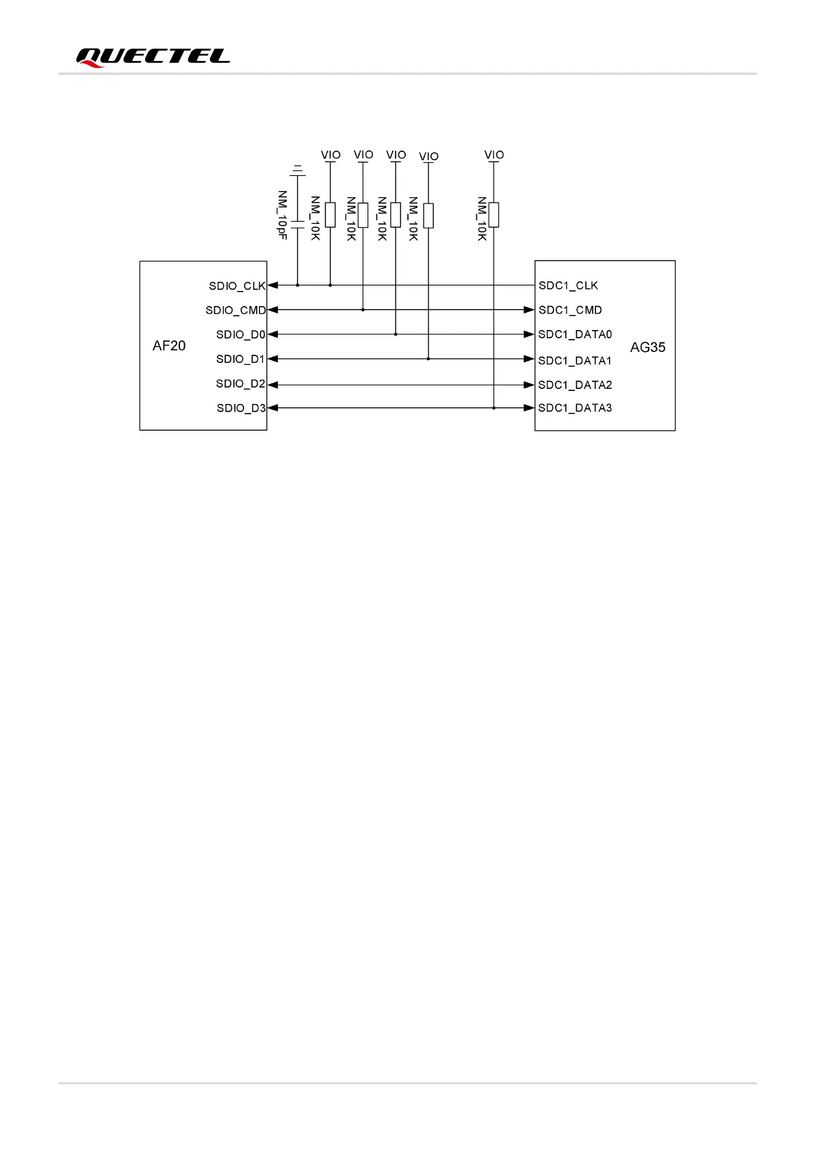
The following figure shows the SDIO interface connection between AF20 and AG35 module.
Figure 6: SDIO Interface Connection
SDIO signals are very high-speed signals. In order to ensure compliance with SDIO 3.0 specification,
please comply with the following principles for SDIO interface design.
Surround the SDIO traces with ground on that layer and with ground planes above and below. The
impedance of SDIO signal trace is 50 Ω ±10 %.
Keep SDIO signals far away from other sensitive circuits/signals such as RF circuits and analog
signals, as well as noisy signals such as clock signals and DC-DC signals.
Keep SDIO traces as parallel as possible in the same layer. Make sure SDIO traces are surrounded
by ground vias and not crossed with each other.
Keep SDIO traces as short as possible with equal length. It is recommended to keep the trace length
difference between SDIO_CLK and SDIO_D[0:3]/SDIO_CMD less than 1 mm and the total routing
length less than 50 mm. The total length of SDIO signal traces inside AG35 module is 12 mm and
that inside AF20 is 10 mm, so the exterior total trace length should be less than 28 mm.
On the SDIO_CLK signal trace, a 15 to 24 Ω terminal matching resistance should be placed near the
AG35 module. The distance between the SDC1_CLK pin of the AG35 module and the matching
resistance should be less than 5 mm.
Make sure that the adjacent trace spacing is not less than twice the trace width and the bus
capacitance is less than 15 pF.
3.6. Bluetooth Application Interface
The following figure shows the block diagram of Bluetooth application interface connection between AF20
and AG35 module.