Wi-Fi&Bluetooth Module Series
AF20_Hardware_Design
28
/ 49
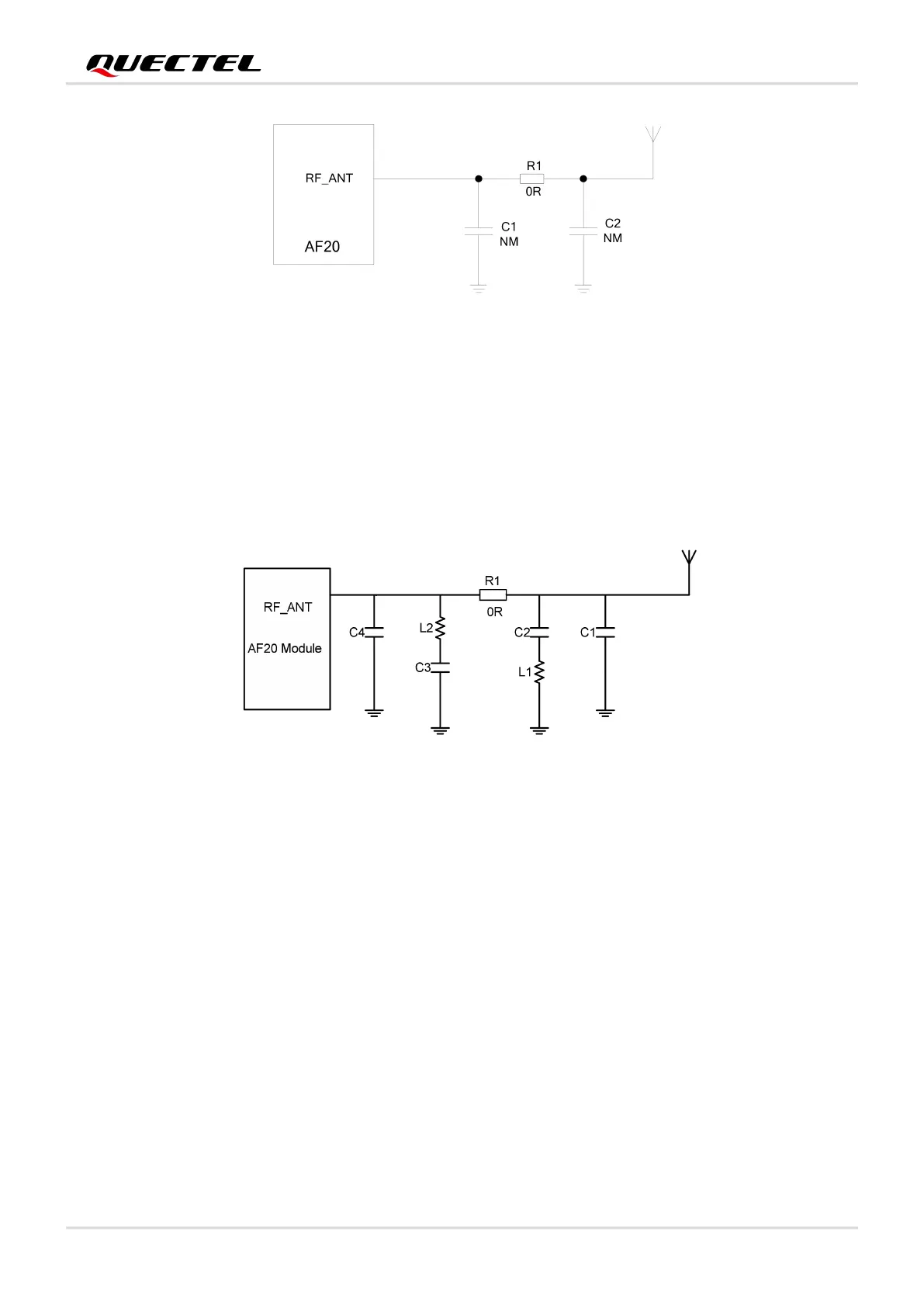
Figure 11: Reference Circuit for RF Antenna Interface
Another type of reference circuit for the RF antenna interface is shown below. It is designed for vehicle
applications. It is recommended to reserve two notch filter circuits and a π-type matching circuit for better
RF performance. C2/L1 and L2/C3 comprise two notch filter circuits for filtering out interference caused by
a particular frequency. When L2/C2/L1/C3 are not mounted, C1/R1/C4 comprise a π-type matching circuit.
Capacitors (C1/C2/C3/C4) and inductors (L1/L2) are not mounted by default, and R1 is only mounted with
0 Ω resistor.
Figure 12: Reference Design of RF Antenna Interface (Vehicle Applications)
3.9.4. RF Routing Guidelines
For user’s PCB, the characteristic impedance of all RF traces should be controlled to 50 Ω. The
impedance of the RF traces is usually determined by the trace width (W), the materials’ dielectric constant,
the height from the reference ground to the signal layer (H), and the spacing between RF traces and
grounds (S). Microstrip or coplanar waveguide is typically used in RF layout to control characteristic
impedance. The following are reference designs of microstrip or coplanar waveguide with different PCB
structures.