Wi-Fi&Bluetooth Module Series
AF20_Hardware_Design
43
/ 49
1. To avoid blistering, layer separation and other soldering issues, extended exposure of the module to
the air is forbidden.
2. Take out the module from the package and put it on high-temperature-resistant fixtures before baking.
If shorter baking time is desired, see IPC/JEDEC J-STD-033 for the baking procedure.
3. Pay attention to ESD protection, such as wearing anti-static gloves, when touching the modules.
6.2. Manufacturing and Soldering
Push the squeegee to apply the solder paste on the surface of stencil, thus making the paste fill the
stencil openings and then penetrate to the PCB. Apply proper force on the squeegee to produce a clean
stencil surface on a single pass. To guarantee module soldering quality, the thickness of stencil for the
module is recommended to be 0.13–0.15 mm. For more details, see document [4].
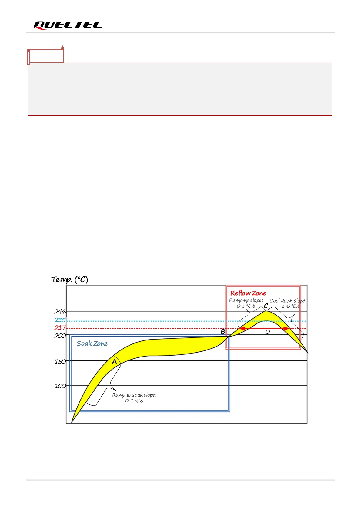
The recommended peak reflow temperature shall be 235–246 ºC, with 246 ºC as the absolute maximum
reflow temperature. To avoid damage to the module caused by repeated heating, it isrecommended that
the module shall be mounted only after reflow soldering for the other side of PCB has been completed.
The recommended reflow soldering thermal profile (lead-free reflow soldering) and related parameters
are shown below.
Figure 24: Recommended Reflow Soldering Thermal Profile