LTE Module Series
EC25 Mini PCIe Hardware Design
EC25_Mini_PCIe_Hardware_Design Confidential / Released 13 / 42
1. “*” means under development.
2.
1)
Within operating temperature range, the module is 3GPP compliant.
3.
2)
Within extended temperature range, the module remains the ability to establish and maintain a
voice, SMS, data transmission, emergency call, etc. There is no unrecoverable malfunction; there are
also no effects on radio spectrum and no harm to radio network. Only one or more parameters like
P
out
might reduce in their value and exceed the specified tolerances. When the temperature returns
to normal operating temperature levels, the module is compliant with 3GPP specification again.
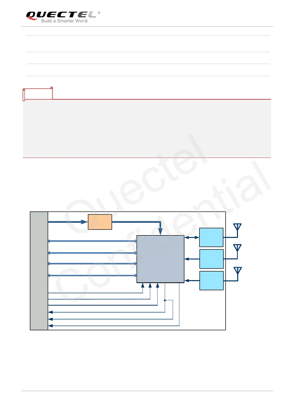
2.4. Functional Diagram
The following figure shows the block diagram of EC25 Mini PCIe.
EC25
Module
PCM&I2C
Mini PCI Express
Interface
USB
USIM
W_DISABLE#
PERST#
LED_WWAN#
Main
Antenna
Interface
VCC
Main
Antenna
VBAT
GNSS
Antenna
Interface
GNSS
Antenna
Boost
Circuit
Diversity
Antenna
Interface
Diversity
Antenna
WAKE#
UART
DTR
RI
Figure 1: Functional Diagram
Operation temperature range: -35°C ~ +75°C
1)
Extended temperature range: -40°C ~ +80°C
2)
All hardware components are fully compliant with EU RoHS directive