LTE Module Series
EC25 Mini PCIe Hardware Design
EC25_Mini_PCIe_Hardware_Design Confidential / Released 24 / 42
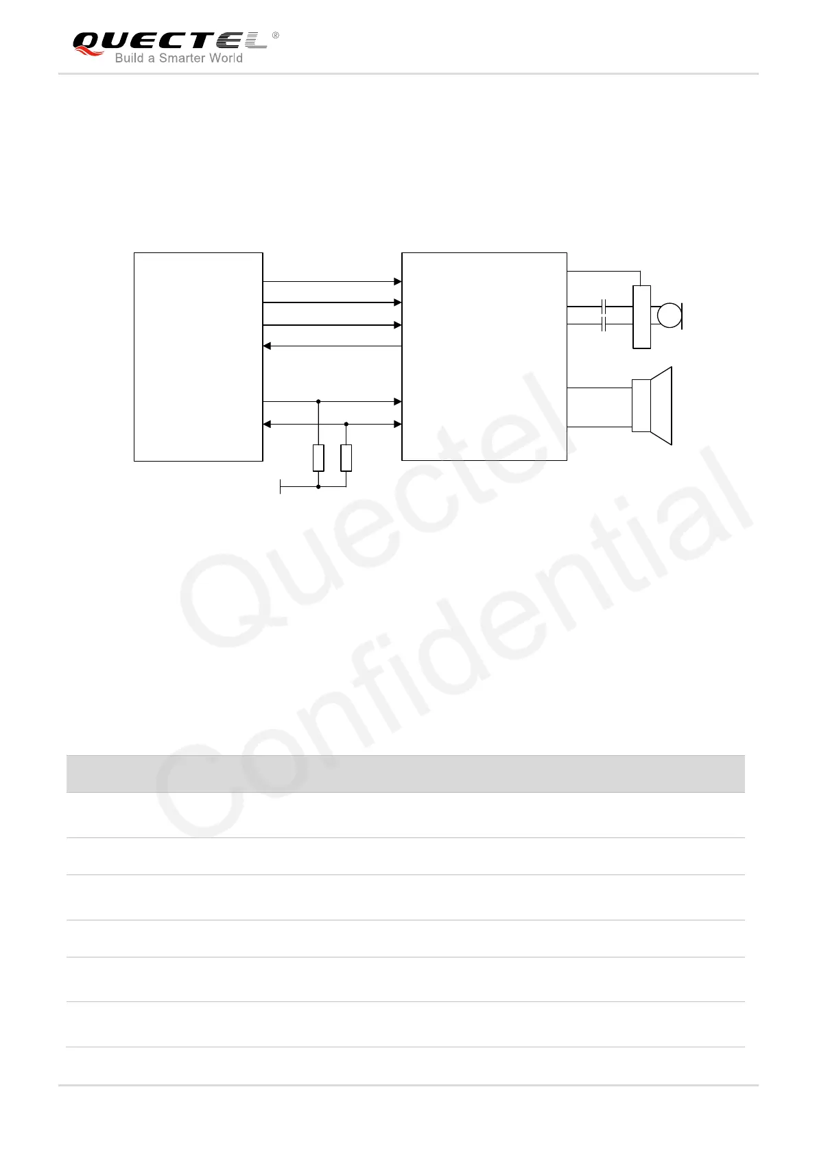
Clock and mode can be configured by AT command, and the default configuration is master mode using
short frame synchronization format with 2048kHz PCM_CLK and 8kHz PCM_SYNC. In addition, EC25
Mini PCIe’s firmware has integrated the configuration on some PCM codec’s application with I2C interface.
Please refer to document [2] for details about AT+QDAI command.
The following figure shows a reference design of PCM interface with an external codec IC.
PCM_DIN
PCM_DOUT
PCM_SYNC
PCM_CLK
I2C_SCL
I2C_SDA
Codec
Module
1.8V
2.2K
2.2K
BCLK
FS
DACIN
ADCOUT
SCLK
SDIN
BIAS
MIC_BIAS
MIC+
MIC-
SPKOUT+
SPKOUT-
Figure 8: Reference Circuit of PCM Application with Audio Codec
3.8. Control Signals
The following table shows the pin definition of control signals.
Table 10: Pin Definition of Control Signals
Output signal can be used to wake up
the host.
Disable wireless communications;
pull-up by default, active low.
Functional reset to the card; active low.
Active-low. LED signal for indicating the
state of the module.
Output signal can be used to wake up
the host.