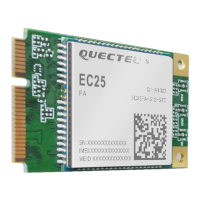
LTE Module Series
EC25 Mini PCIe Hardware Design
EC25_Mini_PCIe_Hardware_Design Confidential / Released 21 / 42
In order to ensure the integrity of USB data line signal, components R1, R2, R3 and R4 must be placed
close to the module, and also these resistors should be placed close to each other. The extra stubs of
trace must be as short as possible.
In order to ensure the USB interface design corresponding with the USB 2.0 specification, please comply
with the following principles:
It is important to route the USB signal traces as differential pairs with total grounding. The impedance
of USB differential trace is 90 ohm.
Do not route signal traces under crystals, oscillators, magnetic devices or RF signal traces. It is
important to route the USB differential traces in inner-layer with ground shielding on not only upper
and lower layers but also right and left sides.
If USB connector is used, please keep the ESD protection components to the USB connector as
close as possible. Pay attention to the influence of junction capacitance of ESD protection
components on USB data lines. Typically, the capacitance value should be less than 2pF.
Keep traces of USB data test points short to avoid noise coupled on USB data lines. If possible,
reserve a 0R resistor on these two lines.
1. There are three preconditions when enabling EC25 Mini PCIe to enter into the sleep mode:
a) Execute AT+QSCLK=1 command to enable the sleep mode. Please refer to document [2] for
details.
b) DTR pin should be kept in high level (pull-up internally).
c) USB interface on Mini PCIe must be connected with the USB interface of the host and please
guarantee the USB of the host is in suspended state.
2. “*” means under development.
3.6. UART Interface
The following table shows the pin definition of the UART interface.
Table 8: Pin Definition of the UART Interface