LTE Standard Module Series
EG91 Series Hardware Design
EG91_Series_Hardware_Design 50 / 106
Table 14: Pin Definition of PCM and I2C Interfaces
Pin Name Pin No. I/O Description Comment
PCM_DIN 6 DI PCM data input 1.8V power domain
PCM_DOUT 7 DO PCM data output 1.8V power domain
PCM_SYNC 5 IO
PCM data frame
synchronization signal
1.8V power domain
PCM_CLK 4 IO PCM data bit clock 1.8V power domain
I2C_SCL 40 OD I2C serial clock Require an external pull-up to 1.8V
I2C_SDA 41 OD I2C serial data Require an external pull-up to 1.8V
Clock and mode can be configured by AT command, and the default configuration is master mode using
short frame synchronization format with 2048KHz PCM_CLK and 8KHz PCM_SYNC. Please refer to
document [2] about AT+QDAI command for details.
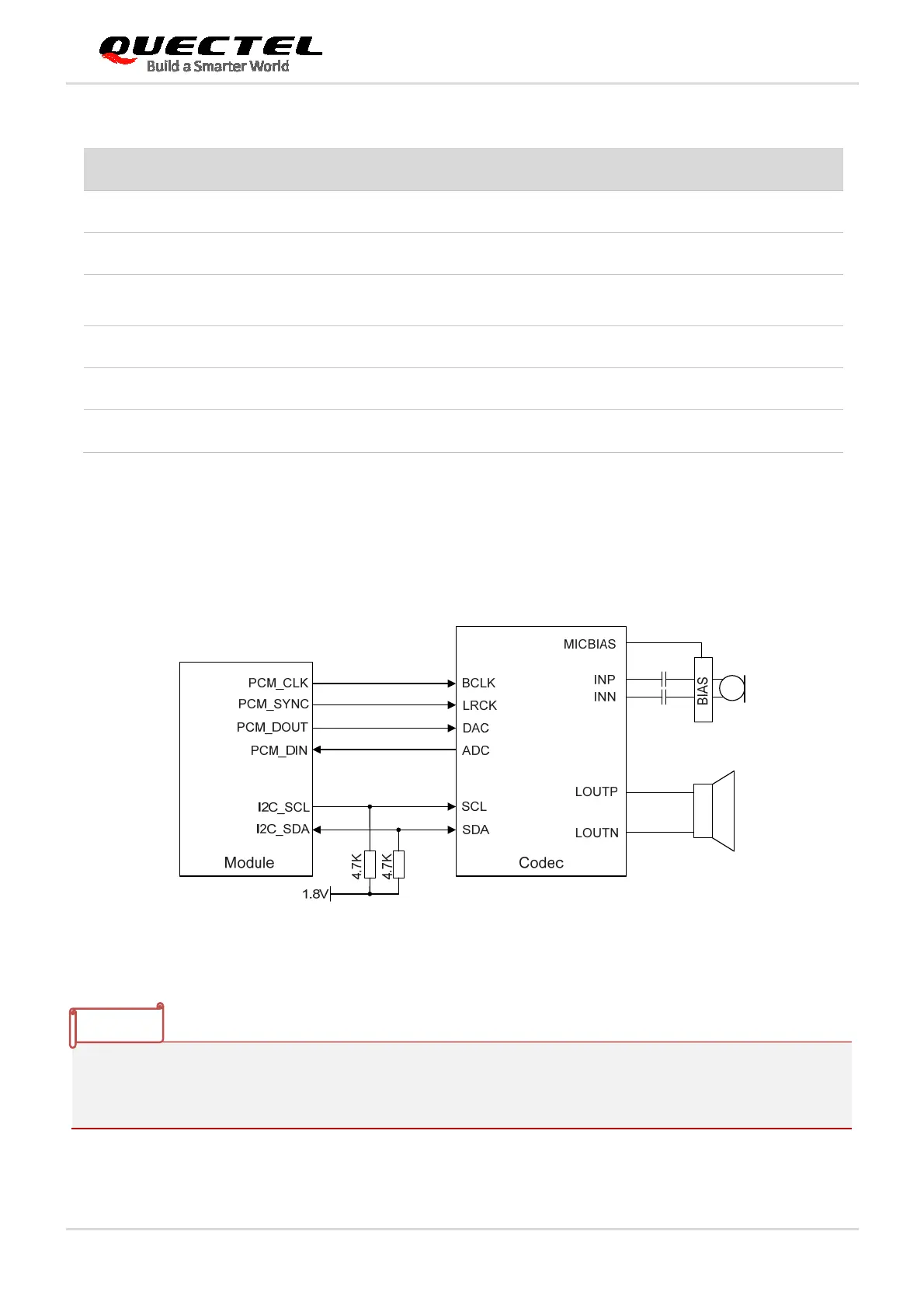
The following figure shows a reference design of PCM interface with external codec IC.
Figure 24: Reference Circuit of PCM Application with Audio Codec
1. It is recommended to reserve an RC (R=22Ω, C=22pF) circuit on the PCM lines, especially for
PCM_CLK.
2. EG91 series module works as a master device pertaining to I2C interface.
NOTES