LTE Standard Module Series
EG915U-EU_Hardware_Design 31 / 81
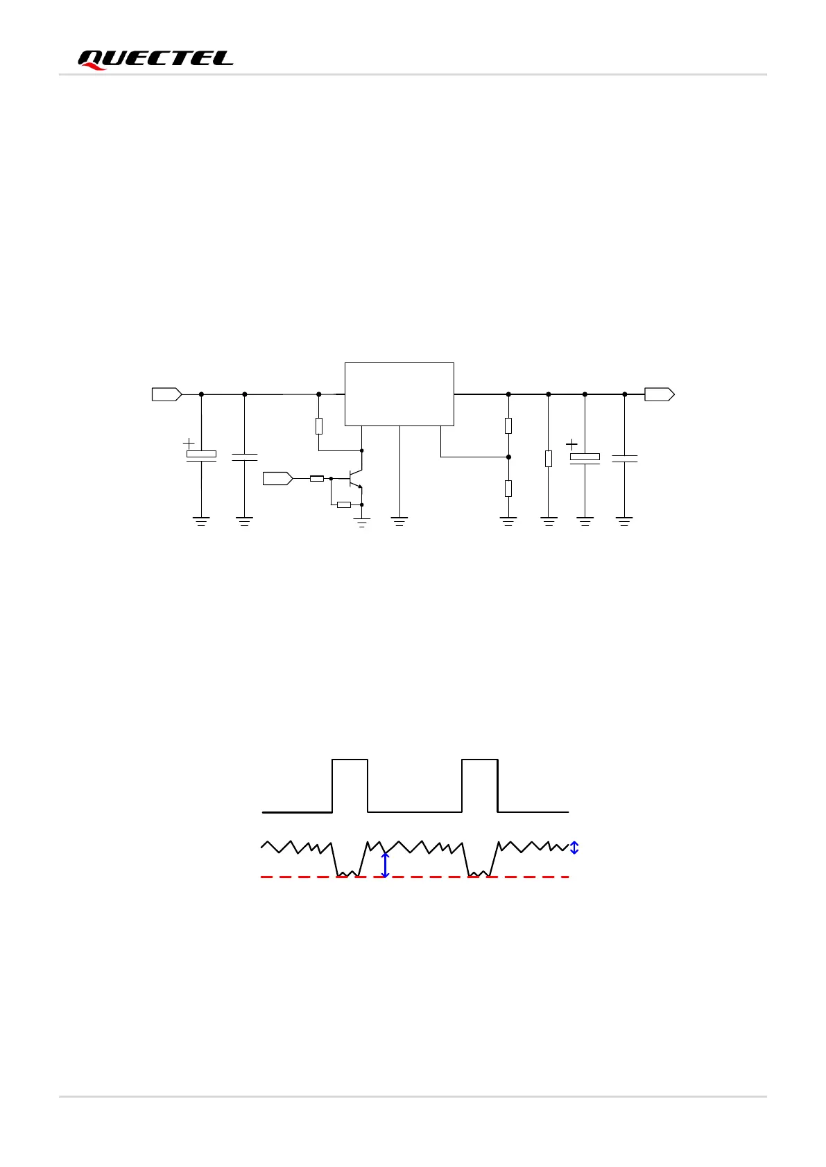
3.4.2. Reference Design for Power Supply
The performance of the module largely depends on the power source. The power supply of the module
should be able to provide sufficient current of 3.0 A at least. If the voltage drops between input and
output is not too high, it is suggested that an LDO should be used to supply power to the module. If
there is a big voltage difference between input and the desired output VBAT, a buck converter is
preferred as the power supply.
The following figure illustrates a reference design for +5 V input power source. The typical output of the
power supply is about 3.8 V and the maximum load current is 3.0 A.
Figure 6: Reference Design of Power Supply
3.4.3. Requirements for Voltage Stability
The power supply range of the module is from 3.3 V to 4.3 V. Please make sure the input voltage will
never drop below 3.3 V.
Figure 7: Power Supply Limits during Burst Transmission
To decrease voltage ‘s drop, a bypass capacitor of about 100 μF with low ESR (ESR = 0.7 Ω) should be
used, and a multi-layer ceramic chip (MLCC) capacitor array should also be reserved due to its ultra-low
ESR. It is recommended to use three ceramic capacitors for composing the MLCC array, and place these
capacitors close to VBAT pins. The main power supply from an external application must be a single
 Loading...