M20 Hardware Design
M20_HD_V1.01 - 64 -
Note: The soldering time for antenna pad and GND pad are different, less than 5s for antenna
pad and less than 10s for GND plan.
4.2 RF output power
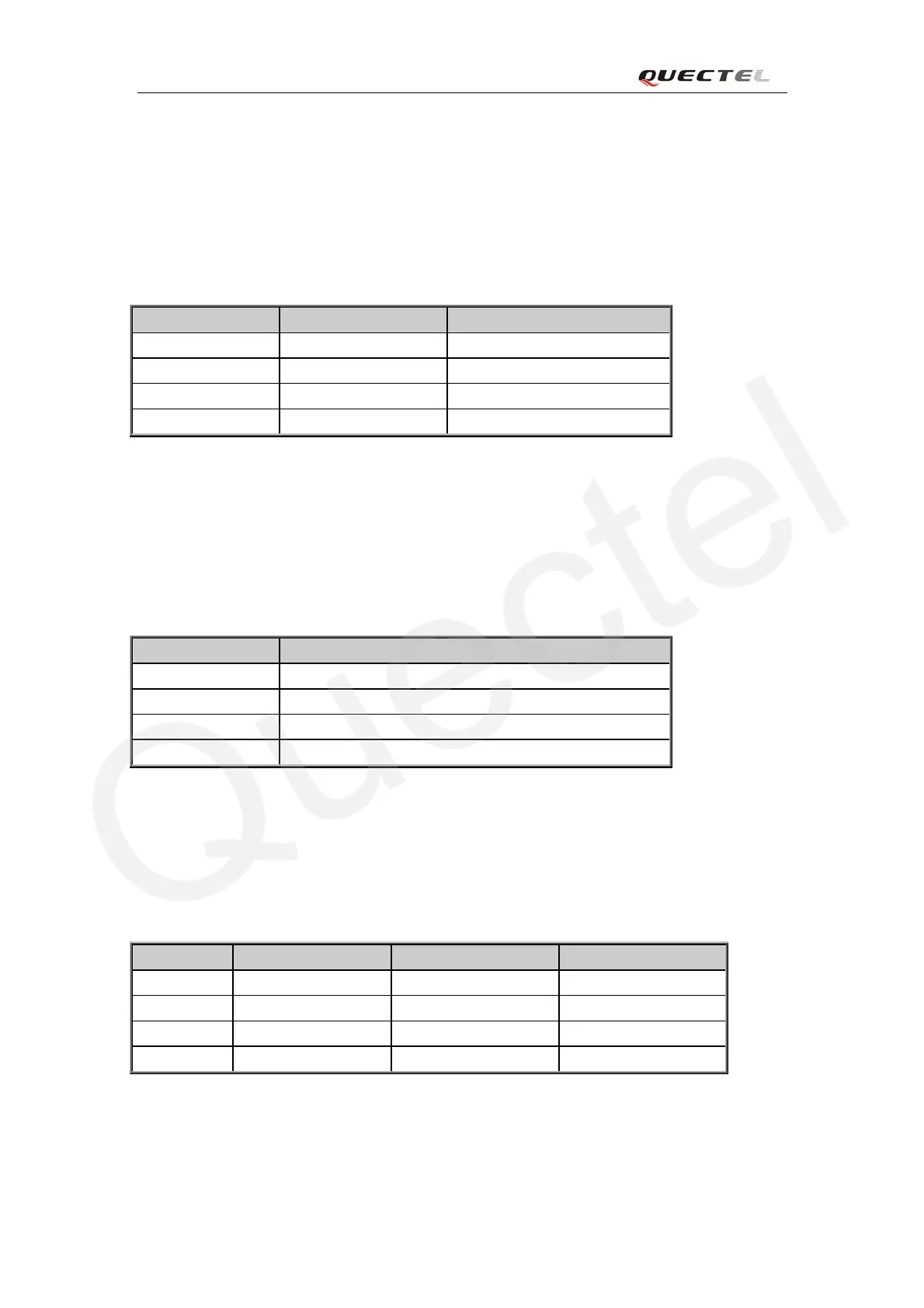
Table 28: The module conducted RF output power
Frequency Max Min
GSM850 33dBm ±2dB 5dBm±5dB
EGSM900 33dBm ±2dB 5dBm±5dB
DCS1800 30dBm ±2dB 0dBm±5dB
PCS1900 30dBm ±2dB 0dBm±5dB
Note: Only in GPRS 4 slots TX mode, the max output power is reduced by 2.5dB.That is
permitted, as described in chapter 13.16 of 3GPP TS 51.010-1.
4.3 RF receiving sensitivity
Table 29: The module conducted RF receiving sensitivity
Frequency Receive sensitivity
GSM850 < -108.7dBm average
EGSM900 < -108.5dBm average
DCS1800 < -108.5dBm average
PCS1900 < -108.1dBm average
Note: The antenna chosen will affect radiated receiving sensitivity.
4.4 Operating frequency
Table 30: The module operating frequency
Frequency Receive Transmit Channel
GSM850 869 ~ 894MHz 824 ~ 849MHz 128 ~ 251
EGSM900 925 ~ 960MHz 880 ~ 915MHz 0~124, 975~1023
DCS1800 1805 ~ 1880MHz 1710 ~ 1785MHz 512 ~ 885
PCS1900 1930 ~ 1990MHz 1850 ~ 1910MHz 512 ~ 810