SIGNAL
SIGNAL
NAME
SIGNAL
SOURCE
FREQUENCY
DIVISION
RATIO
COMMENTS
VDRV
Z32 Pin
11
60.00 Hz 177.3517 X 10
3
Vertical Reference
R8 Z32 Pin 8
60.00 Hz
177.3517 X 10
3
Character
"Row"
R4
Z32 Pin 9
180.0 Hz 59.11722 X 10
3
Character
"R
ow"
R2
Z32 Pin 12
360.0 Hz 29.55861 X 10
3
Character
"Row"
R1
Z65Pin
12
660.0 Hz 16.12288 X 10
3
Character
"R
ow"
l8
Z12Pin11
1.319
kHz
8.067550 X 10
3
Character/Scan
line
l4
Z12Pin8
2.639
kHz
4.032247 X
10
3
Character/Scan
line
l2
Z12Pin9
3.959
kHz
2.687825 X 10
3
Character/Scan Line
l1
Z12Pin
12
7.917kHz
1.344082 X 10
3
Character/Scan
line
HDRV
Z50 Pin
11
15.835
kHz
671.9987
HOrizontal Reference
C32
Z50
Pin 8 31.670
kHz
335.9993 Character Column
C16 Z50 Pin 9
63.340
kHz
167.9997 Character Column
C8
Z50 Pin 12
110.840
kHz
96.00414 Character Column
C4
Z65 Pin 8
221.69
kHz
47.99991 Character Column
C2
Z65 Pin 9
443.38
kHz
23.99995 Character Column
C1
Z43 Pin 7
886.756
kHz
12.0003 NOTE 2
Chain Z43 Pin 9
886.756
kHz
12.0003. Divider Chain
Input
NOTES
1.
All
Frequencies and Division Ratio calculated using 10.641099 MHz (Master
ClK
Frequency
[-0.03%
error]).
2. Signal Frequency shown
is
in 64 character format. Will
be
held
low
in 32 character format.
FIGURE
18.
Table
of
Signal
Frequenciesfor Divider
Chain
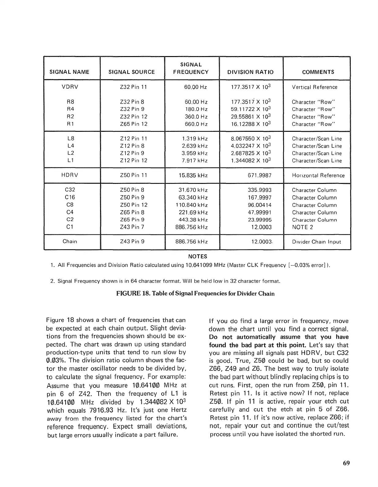
Figure
18
shows
a
chart
of
frequencies
that
can
be
expected
at
each chain
output.
Slight devia-
tions
from
the
frequencies
shown
should
be ex-
pected.
The
chart
was drawn
up
using
standard
production-type
units
that
tend
to
run slow
by
0.03%.
The
division ratio
column
shows
the
fac-
tor
the
master
oscillator needs
to
be divided
by,
to
calculate
the
signal
frequency.
For
example:
Assume
that
you
measure 10.64100 MHz
at
pin 6
of
Z42.
Then
the
frequency
of
L1
is
10.64100 MHz divided
by
1.344082 X 10
3
which equals 7916.93 Hz. It's
just
one
Hertz
away
from
the
frequency
listed for
the
chart's
reference
frequency.
Expect
small deviations,
but
large
errors
usually
indicate
a
part
failure.
If
you
do
find a large
error
in
frequency,
move
down
the
chart
until
you
find a
correct
signal.
Do
not
automatically
assume
that
you
have
found
the
bad
part
at
this
point.
Let's say
that
you
are missing all signals
past
HDRV,
but
C32
is
good.
True,
Z50
could
be bad,
but
so
could
Z66, Z49
and
Z6.
The
best
way
to
truly
isolate
the
bad
part
without
blindly replacing
chips
is
to
cut
runs. First,
open
the
run
from
Z50, pin 11.
Retest
pin 11.
Is
it active
now?
If
not,
replace
Z50.
If
pin
11
is
active, repair
your
etch
cut
carefully
and
cut
the
etch
at
pin 5
of
Z66.
Retest
pin 11. If it's
now
active, replace Z66: if
not,
repair
your
cut
and
continue
the
cutltest
process until
you
have isolated
the
shorted
run.
69
 Loading...