RZ/A2M SUB Board RTK79210XXB00000BE 2. Function specifications
R20UT4398EJ0100 Rev.1.00 2-33
2018.10.11
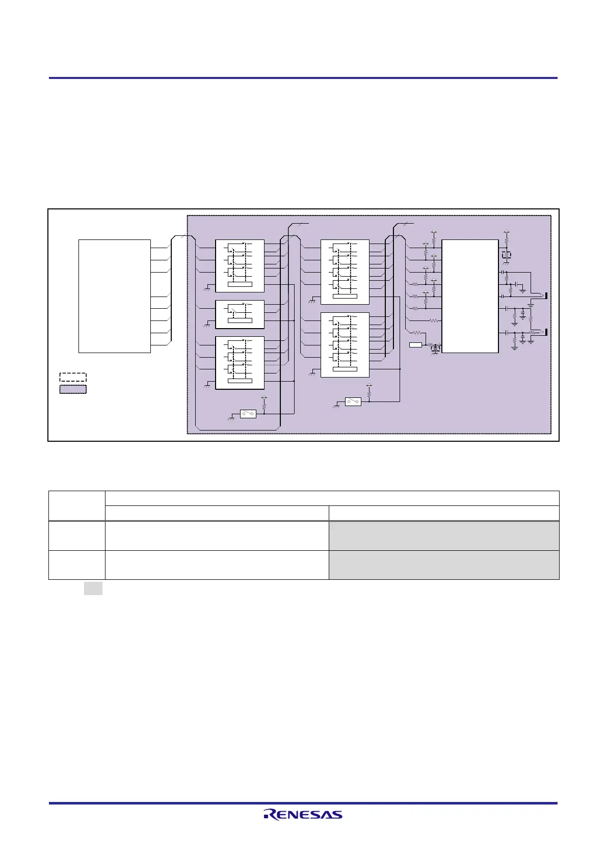
2.10 Audio Interface
RTK79210XXB00000BE is equipped with a Cirrus audio CODEC WM8978 × 1 for audio interface. The WM8978
register control is performed on the channel 0 of the RZ/A2M on-chip Renesas serial peripheral interface (RSPI), and the
input/output control for audio data is performed on the channel 0 of the RZ/A2M on-chip serial sound interface (SSIF-2).
Figure 2.10.1 shows the audio interface block diagram, and Table 2.10.1 shows the function setting table of DIP
switches SW6-1 and SW6-2 for system setting.
Figure 2.10.1 Audio Interface Block Diagram
Table 2.10.1 Function Setting Table of DIP Switches SW6-1 and SW6-2 for System Setting
P8_4 and P8_[7 :6], P9_[6 :3] are used as SDRAM
control pins.
P8_4 and P8_[7 :6], P9_[6 :3] are used as audio
interface pins (default settings).
P8_4 and P8_[7 :6], P6_4, P9_[6 :3] are used as
DRP pins.
P8_4 and P8_[7 :6], P6_4, P9_[6 :3] used as audio
interface pins (default settings).
[Note] indicates setting functions.
P9_4
P9_6
P8_6
P8_4
P9_3
P9_5
P8_7
MOSI
SSL
RSPCK
SSITxD
SSIFS
SSIRxD
SSIBCK
3.3V
3.3V
To DRP I/F
3.3V
3.3V
3.3V
3.3V
P6_4
RZ/A2M (U1)
P8_7 / A7 / DRP17 / RSPCK0
P8_6 / A6 / DRP18 / MOSI0
P8_4 / A4 / DRP20 / SSL00
P9_6 / A14 / DRP10 / SSIBCK0
P9_5 / A13 / DRP11 / SSIFS0
P9_4 / A12 / DRP12 / SSITxD0
P9_3 / A11 / DRP13 / SSIRxD0
P6_4 / DRP00 / AUDIO_CLK
CN4
+
+
Audio CODEC(U21)
BCLK
LRC
ADCDAT
DACDAT
SCLK
SDIN
CSB/GPIO1
MCLK
LOUT1
ROUT1
L2/GPIO2
R2/GPIO3
MICBIAS
CN3
MODE
3.3V
CLK
11.2896MHz
Socket(X1)
SDRAM / Other(Audio)(U10)
P9_4
P9_5
P9_6
SDRAM / Other(Audio)(U8)
P9_3
SDRAM / Other(Audio)(U5)
P8_4
P8_6
P8_7
3.3V
DIP
SW6-1
P6_4
8
7
MUXOE# S
4A
4B1
4B2
MUXOE# S
4A
4B1
4B2
3A
3B1
3B2
1A
1B1
1B2
MUXOE# S
3A
3B1
3B2
2A
2B1
2B2
1A
1B1
1B2
DRP / Audio(U6)
P9_6
P8_6
P8_7
P6_4
3.3V
DIP
SW6-2
8
8
MUXOE# S
4A
4B1
4B2
3A
3B1
3B2
2A
2B1
2B2
1A
1B1
1B2
To SDRAM
OFF
OFF
P9_3
DRP / Audio(U3)
MUXOE# S
4A
4B1
4B2
3A
3B1
3B2
2A
2B1
2B2
1A
1B1
1B2
P8_4
P9_4
P9_5
CLK
SSL
MOSI
RSPCK
SSIRxD
SSITxD
SSIFS
SSIBCK
CLK
P8_4
P8_6
P8_7
P9_3
P9_4
P9_5
P9_6
Note: Red text indicates a function used.
:Indicates a function not implemented.
:Indicates a SUB board.
+
ON(L):A=B1, OFF(H):A=B2
ON(L):A=B1, OFF(H):A=B2
8
 Loading...


