EasyManuals Logo

Renesas RTK79210**B00000BE User Manual

Renesas RTK79210**B00000BE
106 pages
To Next Page IconTo Next Page
To Previous Page IconTo Previous Page
Page #76 background imageLoading...
Page #76 background image
RZ/A2M SUB Board RTK79210XXB00000BE 3. Operating specifications
R20UT4398EJ0100 Rev.1.00 3-16
2018.10.11
3.1.9 LVDS Connector (CN14, CN16)
RTK79210XXB00000BE is equipped with the LVDS connector (CN14) and the back light connector (CN16) for
power supply.
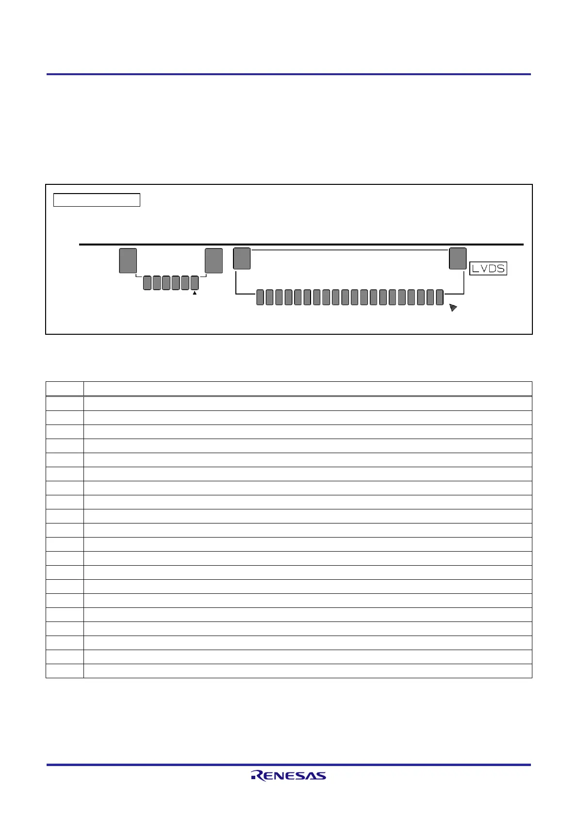
Figure 3.1.12 shows the LVDS connector and LVDS backlight connector pin layout diagram, Table 3.1.12 shows the
LVDS connector pin layout table, and Table 3.1.13 shows the LVDS back light connector pin layout table.
Figure 3.1.12 LVDS Connector (CN14, CN15) Pin Layout Diagram
Table 3.1.12 LVDS Connector (CN14) Pin Layout Table
Pin
Signal name
1
Vcc (+3.3V)
2
Vcc (+3.3V)
3
GND (Vss)
4
GND (Vss)
5
RX0- (P4_1 / TXOUT0M)
6
RX0+ (P4_0 / TXOUT0P)
7
GND (Vss)
8
RX1- (P4_3 / TXOUT1M)
9
RX1+ (P4_2 / TXOUT1P)
10
GND (Vss)
11
RX2- (P4_5 / TXOUT2M)
12
RX2+ (P4_4 / TXOUT2P)
13
GND (Vss)
14
CLK- (P4_7 / TXCLKOUTM)
15
CLK+ (P4_6 / TXCLKOUTP)
16
GND (Vss)
17
L/R or RX3- (connects to +3.3V via 680Ω resistor)
18
U/D or RX3+ (connects to +3.3V via 680Ω resistor)
19
GND (Vss)
20
GND (Vss)
[Note] Red characters indicate functions in use.
120
1
6
CN14
CN16
C side top view

Other manuals for Renesas RTK79210**B00000BE

Questions and Answers:

Question and Answer IconNeed help?

Do you have a question about the Renesas RTK79210**B00000BE and is the answer not in the manual?

Renesas RTK79210**B00000BE Specifications

General IconGeneral
BrandRenesas
ModelRTK79210**B00000BE
CategoryComputer Hardware
LanguageEnglish

Related product manuals