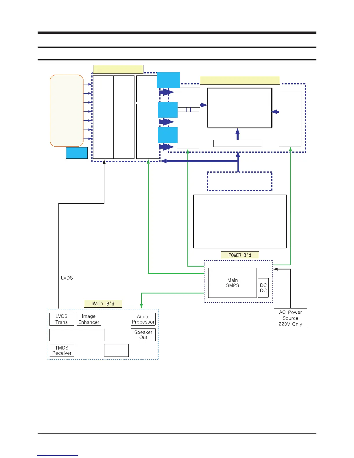
Block Diagram
Samsung Electronics 7-1
7. Block Diagram
7-1 Overall Block Diagram
YPulse
Generator
Row
Driver
Vcc 3V3 Va Vs
Vset Vsc Ve
DRAM
Display
Data
Driver
Timing Controller
Driver
Timing
Scan
Timing
Column Driver
Reference
- 3V3 : Voltage for Logic Control
- Vcc : Voltage for FET driver
- Va : Voltage for address pulse
- Vs : Voltage for sustain pulse
- Vsc : Voltage for scan pulse
- Ve : Voltage for X ramp pulse
- Vset : Voltage for Y ramp pulse
LOGIC CONTROL
DRIVER CIRCUIT & PANEL
Input Data Processor
Data Controller
XPulse
Generator
LVDS
Interface
DCLK
DEN
R-Data
8,10,12 or 13Bits
G-Data
8,10.12 or 13Bits
B-Data
8,10,12 or 13Bits
HSYNC
HSYNC
Micom
Image Scaler +
Video Decoder
852 x 480 Pixels
852 x 3 x 480 Cells