Circuit Description
Samsung Electronics 13-7
■ Requisite Components Necessary for Drive Board Operation
1) Power
- Supplied from the power board. The optimal value may differ from the following:
a) Vs : 200V - Sustain
b) Vset : 190V - Y Rising Ramp
c) Ve : 110V - Ve bias
d) Vscan : -190V - Scan low bias
e) Vsc_h : -70V - Scan high bias (Created by the DC-DC power block of the Y Drive board)
f) Vdd : 5V - Logic signal buffer IC
g) Vcc : 15V - Gate drive IC
2) Logic Signal
- Supplied by the Logic board
- Gate signal of each switch
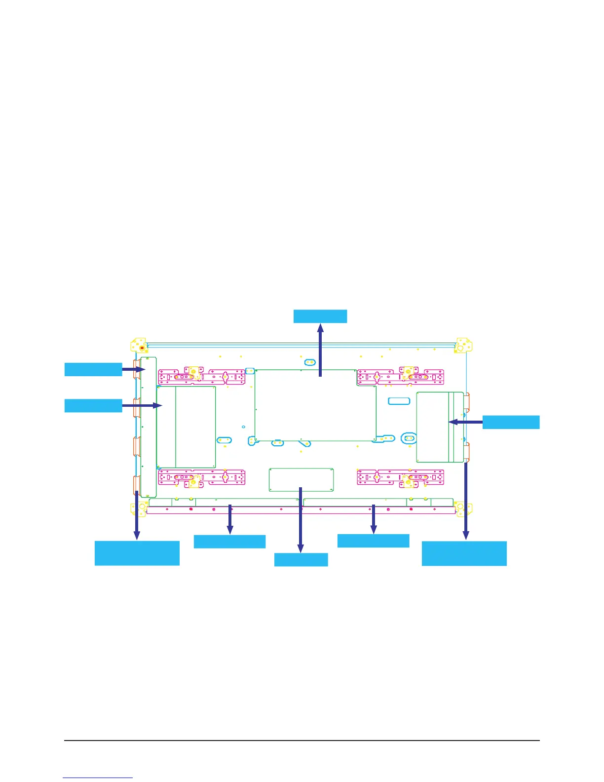
■ Drive Circuit Architecture and Function Description
- Description of the function of each board
1) X Drive Board
This is connected to the X port part of the panel. 1) Sustain voltage waveform (including ERC) is output, and 2) Ve bias in the Scan
section is maintained.
2) Y Drive Board
This is connected to the Y port part of the panel. It outputs 1) Sustain voltage wave form (including ERC), and 2) Y Rising, Falling
Ramp waveform, and maintains 3) Vscan bias.
3) Y Buffer Board
A board, which applies the Scan waveform to the Y terminal block, consists of 12 Scan Driver ICs (TI SN755870: 64 Outputs).