SDP3B FlashDisk Product Manual
SanDisk SDP3B FlashDisk Product Manual © 1998 SANDISK CORPORATION22
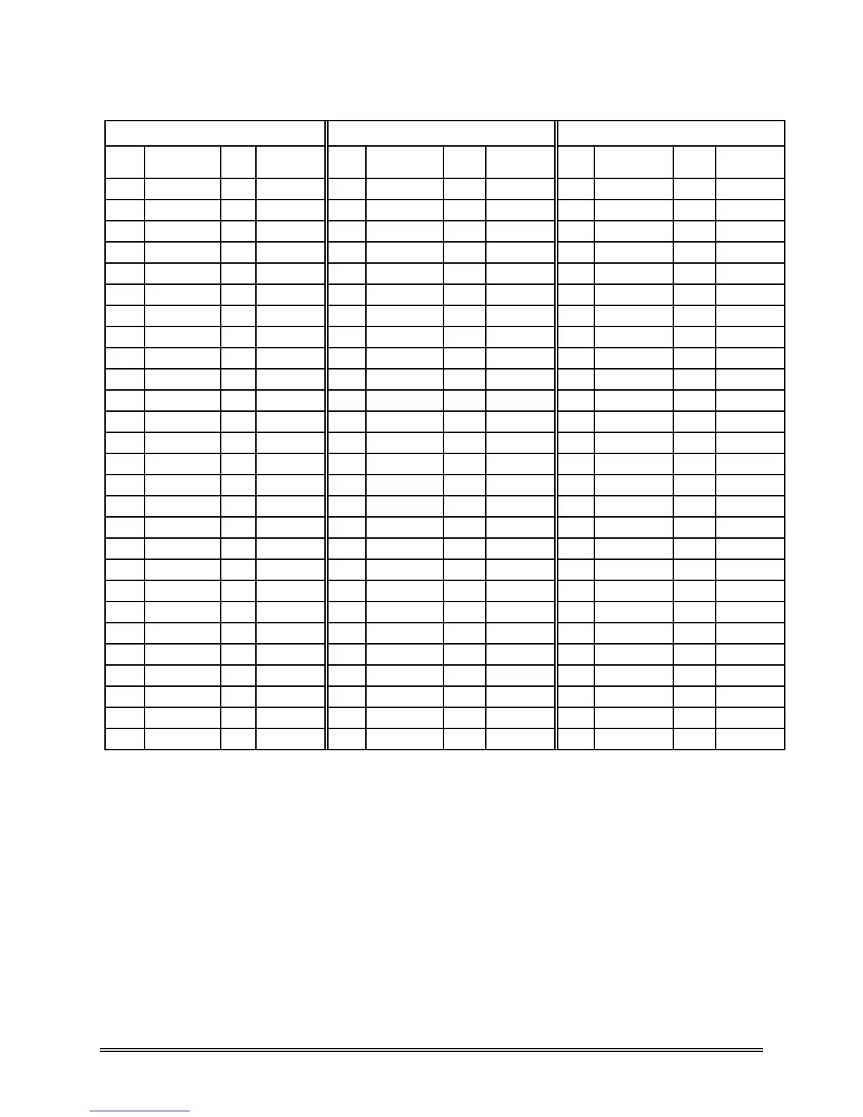
Table 4-1 Pin Assignments and Pin Type (continued)
PC Card Memory Mode PC Card I/O Mode True IDE Mode
Pin
Num
Signal
Name
Pin
Type
In, Out
4
Type
Pin
Num
Signal
Name
Pin
Type
In, Out
4
Type
Pin
Num
Signal
Name
Pin
Type
In, Out
4
Type
42
-CE2
1
I I3U
42
-CE2
1
I I3U
42
-CS1
1
I I3Z
43
-VS1 O Ground
43
-VS1 O Ground
43
-VS1 O Ground
44
-IORD I I3U
44
-IORD I I3U
44
-IORD I I3Z
45 -IOWR I
I3U
45 -IOWR I
I3U
45 -IOWR I
I3Z
46 46 46
47 47 47
48 48 48
49 49 49
50 50 50
51 VCC Power 51 VCC Power 51 VCC Power
52 VPP (Not Used) 52 VPP (Not Used) 52 VPP (Not Used)
53 53 53
54 54 54
55 55 55
56 -CSEL I I2Z 56 -CSEL I I2Z 56 -CSEL I I2U
57 -VS2 O OPEN 57 -VS2 O OPEN 57 -VS2 O OPEN
58 RESET I I2Z 58 RESET I I2Z 58 -RESET I I2Z
59 -WAIT O OT1 59 -WAIT O OT1 59 IORDY O ON1
60 -INPACK O OT1 60 -INPACK O OT1 60 -INPACK O OZ1
61 -REG I I3U 61 -REG I I3U 61 -REG
3
I I3U
62 BVD2 I/O I1U,OT1 62 -SPKR I/O I1U,OT1 62 -DASP I/O I1U,ON1
63 BVD1 I/O I1U,OT1 63 -STSCHG I/O I1U,OT1 63 -PDIAG I/O I1U,ON1
64 D08
1
I/O
I1Z,OZ3
64 D08
1
I/O
I1Z,OZ3
64 D08
1
I/O
I1Z,OZ3
65 D09
1
I/O
I1Z,OZ3
65 D09
1
I/O
I1Z,OZ3
65 D09
1
I/O
I1Z,OZ3
66 D10
1
I/O
I1Z,OZ3
66 D10
1
I/O
I1Z,OZ3
66 D10
1
I/O
I1Z,OZ3
67
-CD2 O Ground
67
-CD2 O Ground
67
-CD2 O Ground
68 GND Ground 68 GND Ground 68 GND Ground
Note: 1. These signals are required only for 16 bit access and not required when installed in 8-bit systems.
For lowest power dissipation, leave these signals open.
2. Should be grounded by the host.
3. Should be tied to VCC by the host.
4. Please refer to section 4.3 for definitions of In, Out type.
 Loading...