Do you have a question about the SanDisk SDSDB-016G-A11 and is the answer not in the manual?
Overview of the SanDisk SD Card's features, design, and compatibility with standards.
Details the key features of the SanDisk SD Card, including storage, protocols, and capabilities.
Information on SD Card compatibility with the SD Card Physical Layer System Specification v1.10.
Describes the intelligent subsystem and capabilities of SanDisk SD cards, including error recovery.
Explains how the SD Card manages flash memory without host intervention.
Details the card's sophisticated system for managing defects and recovering from errors.
Explains the copyright protection mechanism and related SD Card commands.
Discusses the endurance specification for SD Card sectors and typical usage scenarios.
Covers SD Bus mode operations, including standard compliance and identification.
Details the SPI mode protocol, its features, and differences from SD Bus mode.
States that all values are defined at ambient temperature and nominal supply voltage.
Details environmental specifications for the SanDisk SD Card, including temperature, humidity, and ESD.
Lists reliability and durability specifications such as mating cycles, bending, torque, and drop tests.
Provides typical power consumption values for Sleep, Read, and Write operations.
Lists performance values for Block Read/Write Access Time, Power-up, and Sleep to Ready.
Details system reliability specifications like MTBF, preventative maintenance, data reliability, and endurance.
Provides physical specifications and dimensions for the SD Card, including weight, length, width, and thickness.
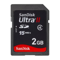
Shows the specific capacity for various SanDisk SD Card models.
Describes the nine exposed contacts on the SD Card and the dedicated 9-pin connector.
Explains the SD Bus topology, including communication lines and supply lines.
Details the SPI Bus topology, including signals like CS, CLK, DataIn, and DataOut.
Covers the electrical interface, including power-up sequences and bus operating conditions.
Introduces the set of registers within the card interface, including OCR, CID, CSD, SCR, RCA, and Status.
Explains the CSD Register's role in storing card configuration information required for data access.
Defines the structure of the SD Card Status Register and its bits.
Describes the SD Status Register, containing bits for proprietary features and future application usage.
Explains the RCA Register's role in carrying the card address for host-card communication.
Details the data structure and card sizes, including user area and security protected areas.
Explains the communication over the SD bus based on command, response, and data bit streams.
Describes how the host controls communication and the two types of commands: Broadcast and Addressed.
Explains the process of identifying cards, validating voltage, and assigning relative addresses.
Covers various aspects of data transfer, including formats, erase, and protection.
Explains how the host controls the SD Card bus clock for energy saving or data flow.
Details Cyclic Redundancy Codes (CRC) used for error detection in commands, responses, and data.
Provides information on various error conditions encountered during SD Card operations.
Lists and describes the various commands used to control the SD Card bus.
Defines the SD card state transitions based on received commands.
Illustrates various timing diagrams for commands, responses, and data transfers.
Explains the process of reading data from the SD Card, including single block operations.
Describes the process of writing data to the SD Card, including single block operations.
Defines various timing values and constants used in SD Card operations.
Explains the SPI bus protocol, its byte-oriented nature, and differences from SD Bus mode.
Describes how the SD Card enters SPI mode and the process of returning to SD Bus mode.
Discusses CRC protection and the non-protected mode in SPI mode.
Details SPI mode data read operations, including single and multiple block transfers.
Describes SPI mode data write operations, including single and multiple block transfers.
States that erase and write protect management procedures in SPI mode are identical to SD Bus mode.
Explains reading CID/CSD registers in SPI mode as a simple read-block transaction.
Details the defined reset sequence for SD Memory Cards in SPI mode, including valid commands.
Explains how SPI hosts can control clock frequency for energy saving or data flow.
Provides information on error conditions encountered in SPI mode, including CRC and illegal commands.
References SD Card Bus Mode for memory array partitioning details.
States that card lock/unlock commands in SPI mode are identical to SD mode.
Notes that application-specific commands are identical to SD mode, except for APP_CMD status bit.
States that copyright protection ACMDs and security functionality are the same as SD Bus mode.
States that Switch Function Command is same as SD mode with two exceptions.
Notes that High-speed Mode is not available in SPI Mode.
Provides information on the SPI Command Set, including format and classes.
Details the types of response tokens in SPI mode, including Formats R1, R1b, R2, R3, R4, R5, and Data Response.
Describes data tokens used for read/write transfers, including their format and length.
Explains the data error token sent when a read operation fails to provide data.
Summarizes status bits and their set/clear conditions in SPI mode.
States that OCR, CSD, and CID registers are accessible in SPI Mode.
Illustrates SPI bus timing diagrams for command, response, and data transfers.
Defines timing constants for SPI bus operations.
States that the SPI Mode electrical interface is identical to the SD Card mode.
References SD Card mode for SPI bus operating conditions.
References SD Card mode for bus timing, noting CS signal timing.
Lists SanDisk SD Card part numbers and their corresponding block sizes.
Provides contact information for SanDisk's corporate headquarters.
Lists U.S. Industrial/OEM sales offices, including regional contacts.
Lists international sales offices across Europe, Northern Europe, Central/Southern Europe, Japan, and Asia/Pacific Rim.
States SanDisk's warranty for products against defects in materials or workmanship for one year.
Outlines the limited warranty terms, waivers, and liability limitations.
Details the conditions required for SanDisk to repair or replace a defective product.
Explains the procedure for obtaining warranty service, including authorization and shipping instructions.
Informs users about state-specific warranty rights and limitations.
States SanDisk's policy against using products in life support systems and lists excluded applications.
Provides application notes for host design considerations related to NAND MMC and SD-based products.
Emphasizes the need to meet SD Card and MultiMediaCard bus timing specifications.
Stresses the criticality of read/write time-out values for data accuracy.
| Brand | SanDisk |
|---|---|
| Model | SDSDB-016G-A11 |
| Category | Storage |
| Type | SD Card |
| Capacity | 16 GB |
| Speed Class | Class 4 |
| Read Speed | Up to 15 MB/s |
| Operating Temperature | -25°C to 85°C |
| Storage Temperature | -40°C to 85°C |
| Weight | 2g |
| Warranty | Limited Lifetime Warranty |
| Compatibility | SDHC-compatible devices |
| Dimensions | 24 mm x 32 mm x 2.1 mm |