Chapter 3 – SD Card Interface Description
Revision 2.2 SD Card Product Manual
© 2004 SanDisk Corporation 3-8 12/08/04
Table 3-5 Host and Bus Capacities
8
Parameter S
mbol Min. Max. Unit Remark
Pull-up resistance R
CMD,
R
DAT
10 100 kΩ Prevents bus floating
Bus signal line capacitance C
L
--- 250 pF f
PP
< 5 MHz, 21 cards
Bus signal line capacitance C
L
--- 100 pF
Signal card capacitance C
CARD
--- 10 pF
f
PP
< 20 MHz, 7 cards
Max. signal line inductance --- --- 16 nH f
PP
<20 MHz
Pull-up resistance inside card (pin 1) R
DAT3
10 90 kΩ May be used for card
detection
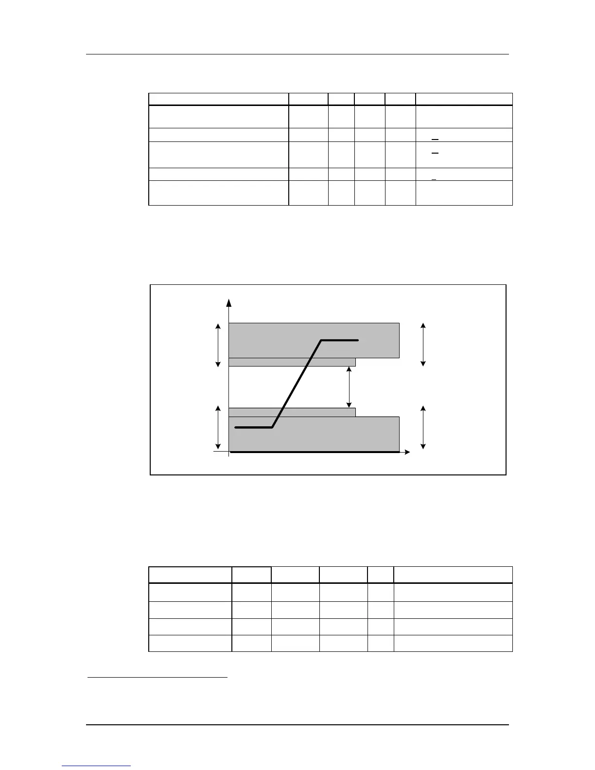
3.4.4 Bus Signal Levels
All signal levels are related to the supply voltage because the bus can have a variable
supply voltage (see Figure 3-6).
Figure 3-6 Bus Signal Levels
3.4.5 Open-drain Mode Bus Signal Level
To meet the requirements of the JEDEC specification JESD8-1A, the card input and output
voltages are within the specified ranges in Table 3-6 for any V
DD
of the allowed voltage
range.
Table 3-6 Input/Output Voltage
Parameter Symbol Min. Max. Unit Conditions
Output high voltage V
OH
0.75*V
DD
--- V I
OH
= -100 uA@ V
DD
(minimum)
Output low voltage V
OL
--- 0.125*V
DD
V I
OL
= 100 uA@ V
DD
(minimum)
Input high voltage V
IH
0.625*V
DD
V
DD
+0.3 V ---
Input low voltage V
IL
V
SS
-0.3 0.25*V
DD
V ---
8
The total capacitance of CMD and DAT lines will consist of C
HOST
, C
BUS
, and one C
CARD
only because they are
connected separately to the SD Card host.
Input
Low
Level
Input
High
Level
Output
High
Level
Output
Low
Level
Undefined
V
DD
V
OH
V
IH
V
L
V
OL
V
SS
t
V
 Loading...