Chapter 3 – SD Card Interface Description
Revision 2.2 SD Card Product Manual
© 2004 SanDisk Corporation 3-13 12/08/04
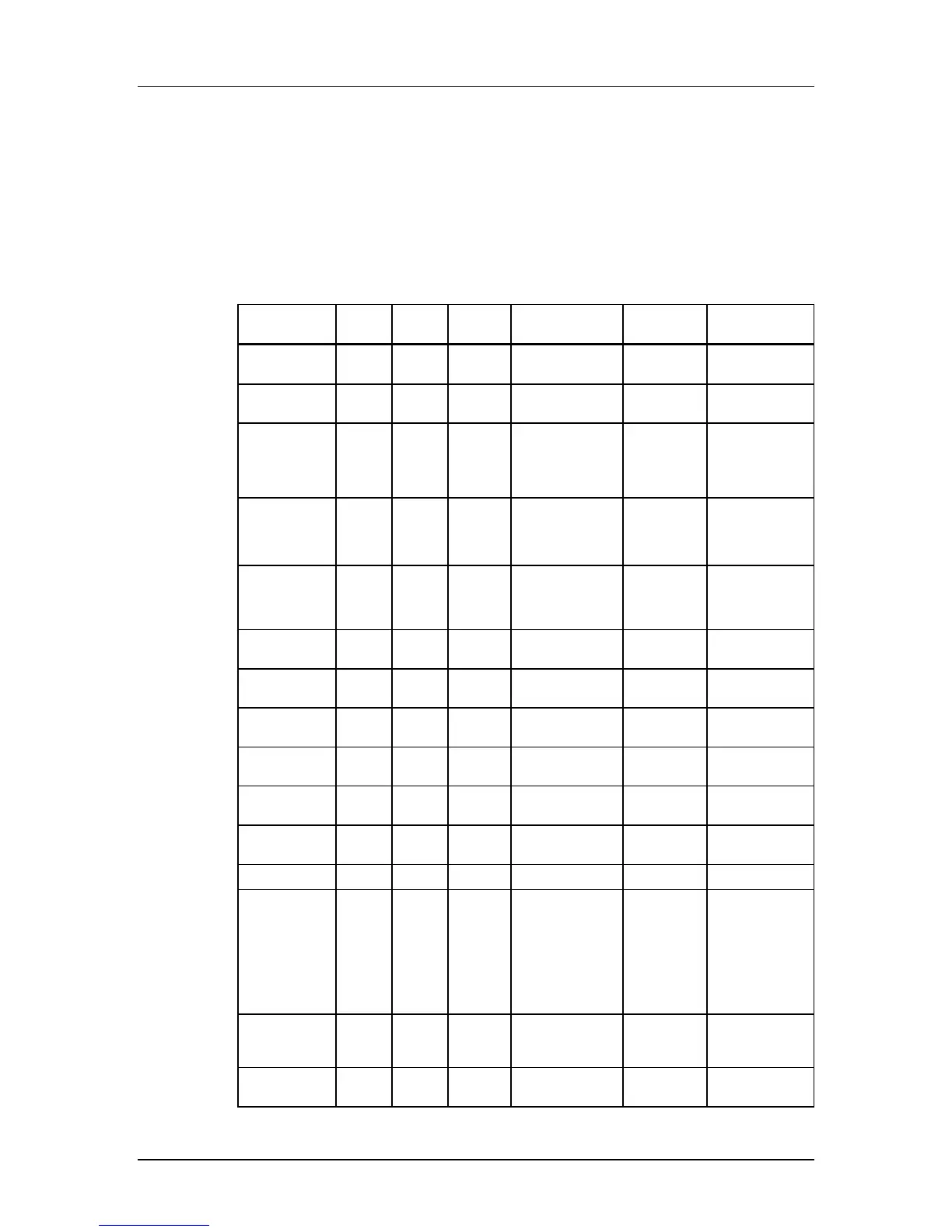
3.5.3 Card Specific Data Register
The Card Specific Data (CSD) Register configuration information is required to access
the card data.
In Table 3-11, the Cell Type column defines the CSD field as read-only (R), one-time
programmable (R/W) or erasable (R/W/E). The values are presented in “real world” units
for each field and coded according to the CSD structure.
Table 3-11 CSD Register Fields
Field Width Cell
Type
CSD
Slice
CSD Value CSD Code Description
CSD_
STRUCTURE
2 R [127:
126]
1.0 0 CSD structure
--- 6 R [125:
120]
--- 000000b Reserved
TAAC
8 R [119:
112]
1.5 msec 00100110 Data read
access time-1
NSAC 8 R [111:
104]
0 00000000b Data read
access time-2 in
CLK cycles
(NSAC*100)
Default 25MHz 0110010 TRANS_
SPEED
8 R [103:96]
High-speed
50MHz
01011010
Max. data
transfer rate
CCC 12 R [95:84] All (inc. WP,
lock/unlock)
5F5 Card command
classes
READ_BL_
LEN
4 R [83:80] 2G
Up to 1G
Ah
9h
Max. read data
block length
READ_BL_
PARTIAL
1 R [79:79] Yes 1b Partial blocks
for read allowed
WRITE_BLK_
MISALIGN
1 R [78:78] No 0b Write block
misalignment
READ_BLK_
MISALIGN
1 R [77:77] No 0b Read block
misalignment
DSR_IMP 1 R [76:76] No 0b DSR
implemented
--- 2 R [75:74] --- 00b Reserved
C_SIZE 12 R [73:62] 2 GB
1 GB
512 MB
256 MB
128 MB
64 MB
32 MB
16 MB
F24h
F22h
F1Eh
F13h
F03h
EDFh
74Bh
383h
Device size
VDD_R_
CURR_MIN
3 R [61:59] 100 mA 111b Max. read
current @VDD
min.
VDD_R_
CURR_MAX
3 R [58:56] 80 mA 110b Max. read
current @VDD
 Loading...