SDP3B FlashDisk Product Manual
SanDisk SDP3B FlashDisk Product Manual © 1998 SANDISK CORPORATION 55
5.5.11 Card (Drive) Address Register
(Address 3F7[377]; Offset Fh)
This register is provided for compatibility with
the AT disk drive interface. It is recommended
that this register not be mapped into the host’s
I/O space because of potential conflicts on Bit 7.
The bits are defined as follows:
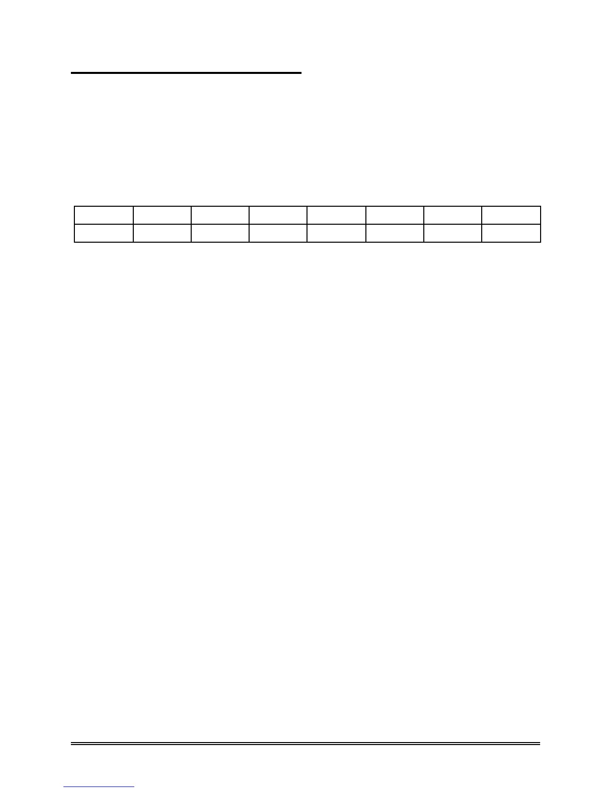
D7 D6 D5 D4 D3 D2 D1 D0
X -WTG -HS3 -HS2 -HS1 -HS0 -nDS1 -nDS0
Bit 7 This bit is unknown.
Implementation Note:
Conflicts may occur on the host data bus when this bit is provided by a Floppy Disk Controller
operating at the same addresses as the SDP3B FlashDisk. Following are some possible solutions
to this problem for the PCMCIA implementation:
1. Locate the SDP3B FlashDisk at a non-conflicting address, i.e. Secondary address (377) or in an
independently decoded Address Space when a Floppy Disk Controller is located at the Primary
addresses.
2. Do not install a Floppy and a SDP3B FlashDisk in the system at the same time.
3. Implement a socket adapter which can be programmed to (conditionally) tri-state D7 of I/0
address 3F7/377 when a SDP3B FlashDisk is installed and conversely to tri-state D6-D0 of I/O
address 3F7/377 when a floppy controller is installed.
4. Do not use the SDP3B FlashDisk 's Drive Address register. This may be accomplished by either
a) If possible, program the host adapter to enable only I/O addresses 1F0-1F7, 3F6 (or 170-177,
176) to the SDP3B FlashDisk or b) if provided use an additional Primary / Secondary configuration
in the SDP3B FlashDisk which does not respond to accesses to I/O locations 3F7 and 377. With
either of these implementations, the host software must not attempt to use information in the Drive
Address Register.
Bit 6 (-WTG) This bit is 0 when a write operation is in progress, otherwise, it is 1.
Bit 5 (-HS3) This bit is the negation of bit 3 in the Drive/Head register.
Bit 4 (-HS2) This bit is the negation of bit 2 in the Drive/Head register.
Bit 3 (-HS1) This bit is the negation of bit 1 in the Drive/Head register.
Bit 2 (-HS0) This bit is the negation of bit 0 in the Drive/Head register.
Bit 1 (-nDS1) This bit is 0 when drive 1 is active and selected.
Bit 0 (-nDS0) This bit is 0 when the drive 0 is active and selected.