Signal Pin Numbers Description
SDIS/DMAK2 27 General purpose output pin.
SDOUT 20 Sigma-Delta Data Out —
Input to the SDC analog
transmitter.
SEL0 108 Zone Select — Used to
adderss the device according
to the selected zone.
SEL1 110
SEL3 107
SLS 21 General purpose output pin.
SMPH0 ∼ 3 70 69 68
67
Output port.
SOSCO 63 Low-Speed Oscillator Out —
Asynchronous. This line is
used as the return path for
the crystal (if used).
SPDW 23 General purpose output pin.
STB0-3 35 34 31
30
General purpose output pin.
WDT 60 WATCHDOG Trap — Traps
CPU execution when
WATCHDOG detects error.
WEO 113 Write Enable — Used by the
addressed device to get the
data from the data bus.WE0
for even and WE1 for odd
bytes.
WE1 112
Input/Output Signals
Signal Pin Numbers Description
A16 ∼ 23 7 8 9
10 12 13
14 15
High Order Address Bus —
The most significant eight bits
of the CPU address bus.
AD0 ∼ 15 120 121 122
123 124 126
127 128 129
130 132 1
2 3 4
6
Address/Data bus —
Multiplexed address/data
information.
ADS 118 Address Strobe — Controls
memory access, and signals
the beginning of a bus cycle.
DDIN 119 Data Direction In —
Indicates the direction of data
transfer during a bus cycle.
MWSO 47 General purpose I/O pin.
PCLK/DMRQ1 49 General purpose I/O pin.
PIO0-1 54 53 General Purpose I/O Pins.
SBYPS/DMRQ2 48 General purpose I/O pin.
SNH/DMRQ0 52 Sample and Hold — Output
to scanner sample and hold
circuit or DMA Request-input
for DMA channel 0 reques.
UREN 45 General purpose I/O pin.
UTXD 46 UART Transmit — Output.
(2) NS32FX164 (IC507)
Supplles
V
CC
Power
+5 V positive supply.
GND Ground.
Ground reference for both on-chip logic and output
drivers.
Input Signals
RSTI Reset Input.
Schmitt triggered, asynchronous signal used to generate a
CPU reset.
Note: The reset signal is a true asynchronous input.
Therefore, no external synchronizing circuit is
needed.
HOLD Hold Request.
When active, causes the CPU to release the bus for DMA
or multiprocessing purposes.
Note: If the HOLD signal is generated asynchronously, its
set up and hold times may be violated. In this case,
it is recommended to synchronize it with CTTL to
minimize the possibility of metastable states.The
CPU provides only one synchronization stage to
minimize the HLDA latency. This is to avoid speed
degradations in cases of heavy HOLD activity (i.e.,
DMA controller cycles interleaved with CPU
cycles).
INT Interrupt.
A low level on this pin requests a maskable interrupt. INT
must be kept asserted until the interrupt is acknowledged.
NMI Non-Maskable Interrupt.
A High-to-Low transition on this signal requests a non-
maskable interrupt.
Note: INT and NMI are true asynchronous inputs. There-
fore, no external synchronizing circuit is needed.
CWAIT Continuous Walt.
Causes the CPU to insert continuous wait states if
sampled low at the end of T2 and each following T-State.
OSCIN Crystal/External Clock Input.
Input from a crystal or an external clock source.
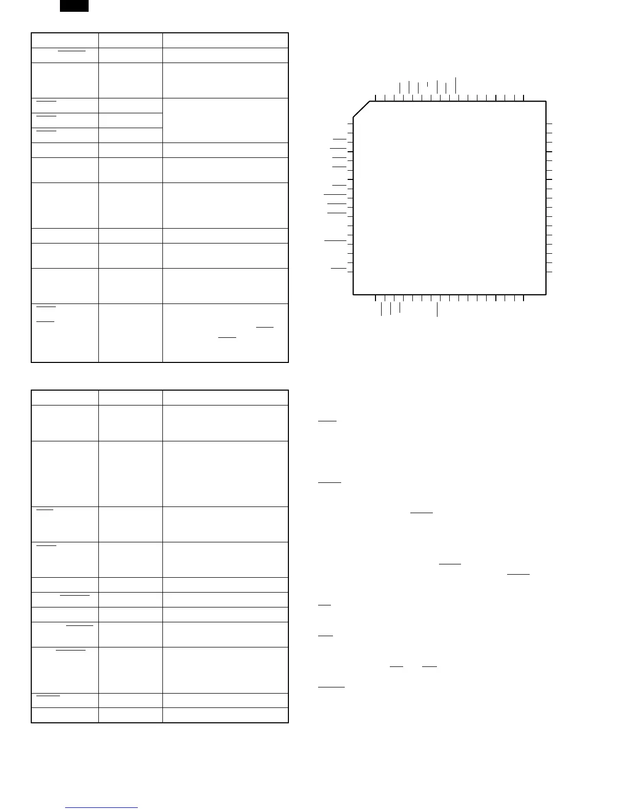
9
ST2
8
ST3
7
PFS
6
DDIN
5
ADS
4
SPC
3
VCC
2
HBE
1
HOLDA
68
HOLD
67
RSTO
66
RES
65
RES
64
CWAIT
63
GND
62
OSCIN
61
RSTI
27 A18
28 A17
29 A16
30
VCC
31
AD15
32
AD14
33
AD13
34
AD12
35
AD11
36
AD10
37
AD9
38
AD8
39
GND
40
AD7
41
AD6
42
AD5
43
AD4
10
GND
11
ST1
12
ST0
13
ILO
14
NMI
15
INT
16
U/S
17
BPU
18
IAS
19
IOUT
20
VCC
21
A23
22
A22
23
A21
24
A20
25
A19
26
GND
60
OSCOUT
59
TSO
58
WR
57
RD
56
GND
55
CTTL1
54
VCC
53
DBE
52
GND
51
VCC
50
CTTL2
49
FCLK
48
ALE
47
AD0
46
AD1
45
AD2
44
AD3
NS32FX164
NS32FV16
NS32FX161
68-Pin PCC Package
AR-F152
12 – 15