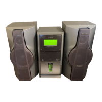
CD-CH1000
– 56 –
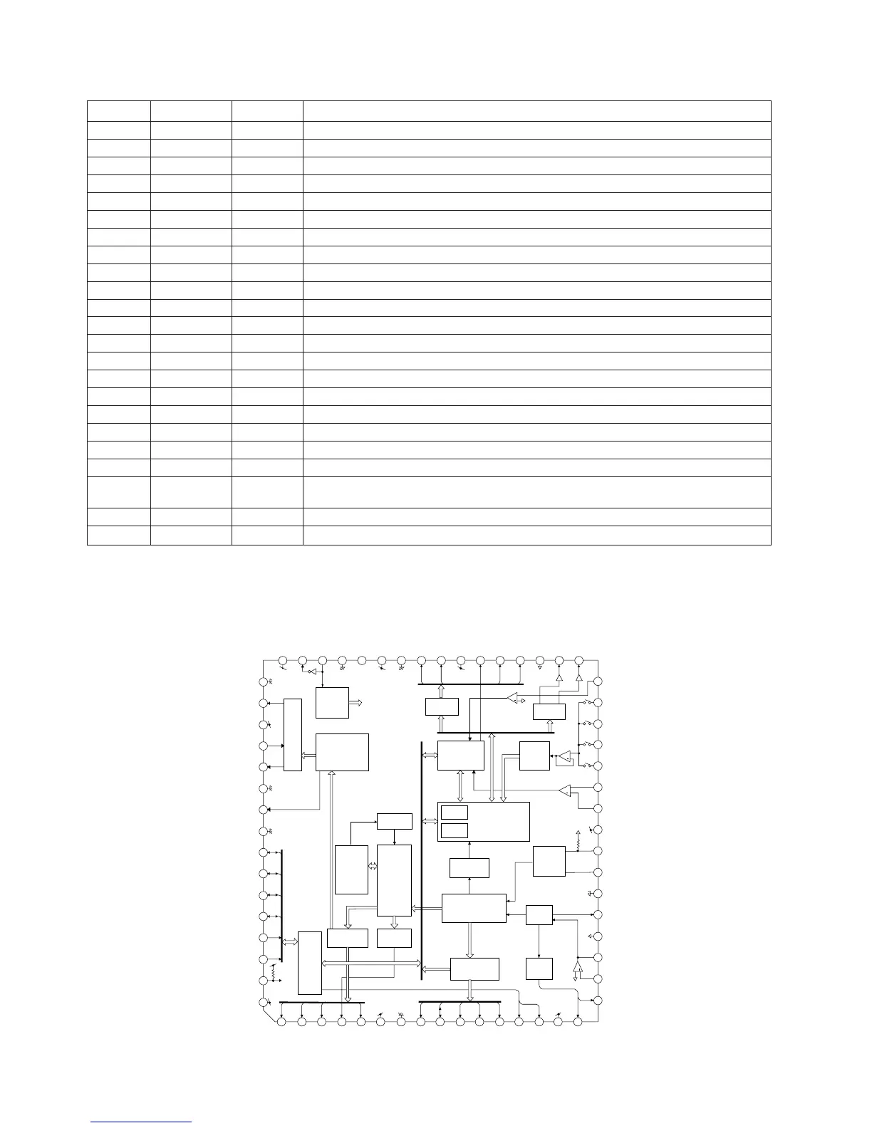
IC2 VHiTC9490F/-1: Servo/Signal Control (TC9490F) (2/2)
39 AVDD3 — Analog 3.3V power supply terminal.
40 FMO Output Feed equalizer output terminal.
41 DMO Output Disc equalizer output terminal.
42 VSS3 — Digital GND terminal.
43 VDD3 — Digital 3.3V power supply terminal.
44 TESIN Input Test input terminal. Usually "L" fixed.
45 XVSS3 — GND terminal for system clock oscillation circuit.
46 XI Input System clock oscillation circuit input terminal.
47 XO Output System clock oscillation circuit output terminal.
48 XVDD3 — 3.3V power supply terminal for system clock oscillation circuit.
49 DVSS3 — GND terminal for D/A converter.
50 RO Output R channel data normal rotation output terminal.
51 DVDD3 — 3.3V power supply terminal for D/A converter.
52 DVR — Reference voltage terminal.
53 LO Output L channel data normal rotation output terminal.
54 DVSS3 — D/A converter section GND terminal.
55* ZDET Output 1-bit D/A converter 0 detection flag output terminal.
56 VSS5 — GND terminal for microcomputer interface.
57-60 BUS0-BUS3 Input/Output Data input/output terminal for microcomputer interface.
61 BUCK Input Clock input terminal for microcomputer interface.
62 /CCE Input Chip enable signal input terminal for microcomputer interface.
In case of "L", BUS3-0 are active.
63 /RST Input Reset signal input terminal. Reset: "L".
64 VDD5 — 5V power supply terminal for microcomputer interface.
Pin No.
Terminal Name
Function
Input/Output
In this unit, the terminal with asterisk mark (*) is (open) terminal which is not connected to the outside.
Note:
AI/F: Analog input/output terminal
3-5I/F: Terminal with a built-in 3-5 interface (5V system input/output terminal)
3I/F: 3V system input/output terminal
Figure 56 BLOCK DIAGRAM OF IC
XVDD3
XO
XI
XVSS3
TESIN
VDD3
VSS3
DMO
FMO
AVDD3
SEL
TEBC
RFGC
VREF
TRO
FOO
TEZI
TEI
SBAD
FEI
RFRP
RFZI
RFCT
AVDD3
RFI
SLCO
AVSS3
VCOF
PVREF
LPFO
LPFN
TMAX
PDD
PVDD3
/HSO
/UHSO
SBSY
SFSY
DATA
CLCK
SBOK
VSS3
VDD3
IPF
DOUT
AOUT
LRCK
BCK
DVSS3
RO
DVDD3
DVR
LO
DVSS3
ZDET
VSS5
BUS1
BUS2
BUS3
BUCK
/CCE
/RST
VDD5
1
23
4
56
7
8
9
10
11
12
13
14
15 16
17
18
19
20
21
22
23
24
25
26
27
28
29
30
31
32
33
3435
36
37
38
39
40
41
4243
44
4546
47
48
49
50
51
52
53
54
55
56
57
58
59
60
61
62
63
64
LPF
1-bit
DAC
PWM
D/A
A/D
VCO
ROM
RAM
16K RAM
PLL
TMAX
+
+
+
+
BUS0
Clock
generator
Servo control
Digital equalizer
adjustment circuit
Data
slicer
CLV
servo
Synchronizing
signal guarantee
EFM demodulation
Sub-code
demodulation
circuit
Address
circuit
Correction
circuit
Digital
out
Audio output
circuit
Microcomputer
interface