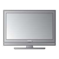
LC-19D1E/S-BK/WH
5 – 6
2.3. IC303 (VHiBD5426MU-1Y)
2.3.1 Block Diagram
2.3.2 Pin Connections and short description
STERO-POWER-AMP.
4 NC - No Connction
5 VOUT O Voltage Output pin with ON/OFF control. (150mA)
Pin No. Pin Name I/O Pin Function
1 BSP2P I ch2 The plus side boost strap terminal 2P (Lch+)
2 VCCA - Analog system power supply terminal
3 FILP I PWM system bias terminal
4 FILA I Analog system bias terminal
5 GNDA - Analog signal system ground terminal
6 IN2 I ch2 analog-signal input terminal (Lch+)
7 IN1 I ch1 analog-signal input terminal (Rch+)
8 PLMT1 I The voltage and the current conversion terminal 1 for an output power- limitation function
9 PLMT2 I The voltage and the current conversion terminal 2 for an output power- limitation function
10 PLMT3 I The voltage and the current conversion terminal 3 for an output power- limitation function
11 PLMT4 I The voltage and the current conversion terminal 4 for an output power- limitation function
12 BSP1P I ch1 The plus side boost strap terminal 1P (Rch+)
13 N.C. - No connection
14 VCCP1P - ch1 Power supply terminal of the plus side power amplifier output (Rch+)
15 VCCP1P - ch1 Power supply terminal of the plus side power amplifier output (Rch+)
16 OUT1P O ch1 Plus side PWM signal output terminal (Rch+)
17 OUT1P O ch1 Plus side PWM signal output terminal (Rch+)
18 GNDP1 - ch1 Ground terminal of a power amplifier output (Rch)
19 GNDP1 - ch1 Ground terminal of a power amplifier output (Rch)
20 OUT1N O ch1 Minus side PWM signal output terminal (Rch-)
21 OUT1N O ch1 Minus side PWM signal output terminal (Rch-)
22 VCCP1N - ch1 Power supply terminal of the minus side power amplifier output (Rch-)
Pin
No.
Pin Name I/O Pin Function