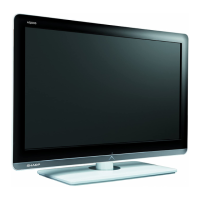
LC-19D1E/S-BK/WH
5 – 18
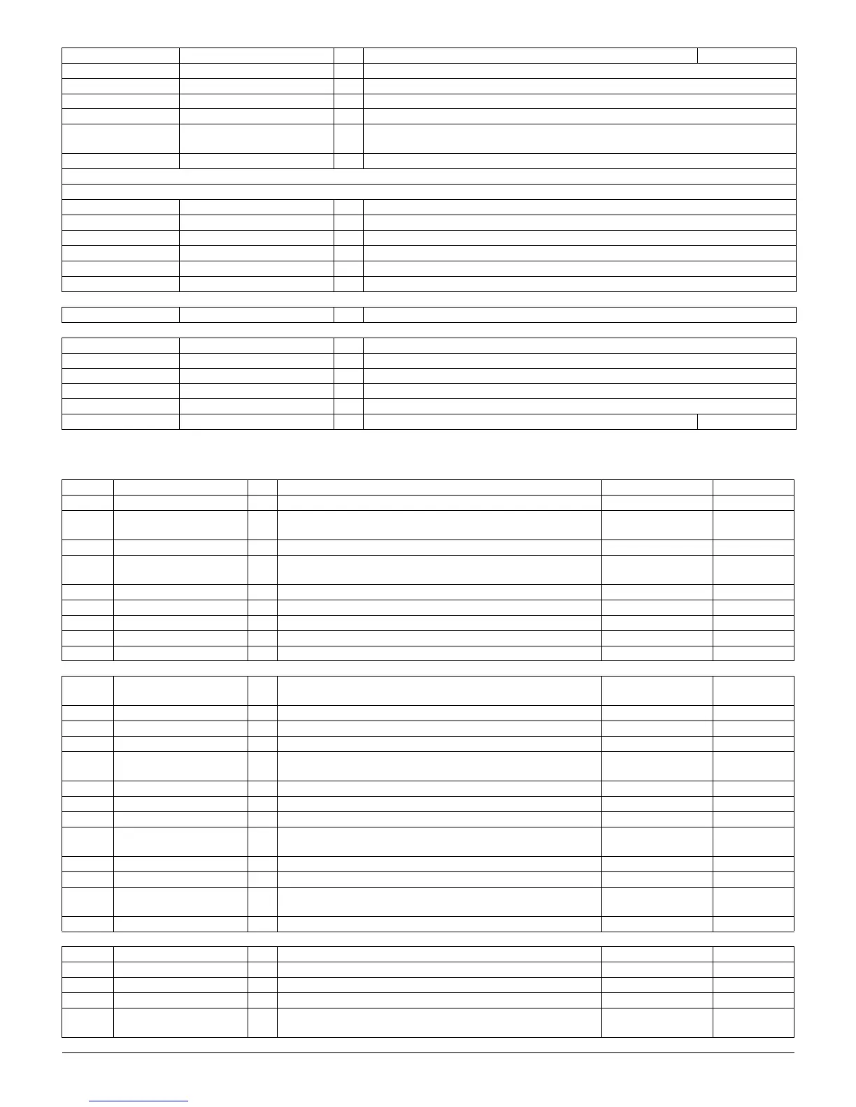
Peripherals
Asynchronous serial controller(ASC)
164 NOT_LMICAS O Latch column address strobe NLMICASBE
206 LMICLKEN O Clock enable LMICLKENBE
203 LMICLKEN O Clock LMICLKBE
202 NOT_LMICLK O inverted clock(DDR). Not used when SDR connected to LMI LMINCLKBE
183 LMI_VREF I Input reference voltage (DDR). Connected to ground when SDR
is connected to LMI.
LMIVREF
166 LMIRDNOTWR O Write enable signal. LMIRDNWRBE
Audio INTERFACE
Analog audio DAC pins
28 OUTLMINUS O Audio DAC left differential current output RIGHTM
24 OUTRMINUS O Audio DAC right differential current output LEFTM
29 OUTLPLUS O Audio DAC left differential current output RIGHTP
25 OUTRPLUS O Audio DAC right differential current output LEFTP
23 VBGOUT O Audio DAC filtered output reference voltage C-GND
26 IREFDAC I Current reference for Audio DAC R-GND
Digital audio pins
37 S/PDIF O Digital audio TL
Video interface
15 VDAC1OUT O Video DAC output 1 R
16 VDAC2OUT O Video DAC output 2 G
17 VDAC3OUT O Video DAC output 3 B
18 VDAC4OUT O Video DAC output 4 CVBS
14 GNDREXTVDAC I Video DAC external resister ground GND
13 REXTVDACRGB I VDAC external resister input R-GND
pin Alternative function I/O Description Usual assignment sheet name
126 ASC0_NOTOE O ASC0_NOTOE PIO0[6] TSSWITCH
118 ASC0_TXD O ASC0 transmit data signal PIO0[0] CARDVC-
COC
119 ASC0_RXD I ASC0 receive data signal PIO0[1] VCCEN
122 ASC0_RTS O ASC0 request to send signal PIO0[4] NOTRE-
SETCI
123 ASC0_CTS I ASC0 clear to send signal PIO0[5] NOTREADY
108 ASC1_TXD O ASC1 transmit data signal PIO2[0] TXD1
109 ASC1_RXD I ASC1 receive data signal PIO2[1] RXD1
110 ASC1_RTM O ASC1 request to send signal PIO2[2] IRQ
111 ASC1_CTS I ASC1 clear to send signal PIO2[3] TL
Smartcards pin mapping
122 SC0_RESET SC0 reset signal PIO0[4] NOTRE-
SETCI
123 SC0_COMD_VCC SC0_command_VCC PIO0[5] NOTREADY
126 SC0_DIR SC0_directry PIO0[6]
127 SC0_DETECT SC0_detection PIO0[7] FERESET
118 SC0_DATAOUT Serial data output PIO0[0] CARDVC-
COC
119 SC0_DATAIN Serial data input PIO0[1] VCCEN
120 SC0_CG_EXTCLK External clock PIO0[2] TL
121 SC0_CG_CLK Clock for smartcard from system clock PIO0[3] FLASHWP
122 SYSRV_SC_RESET_0 Reset to card PIO0[4] NOTRE-
SETCI
123 SYSRV_SC_POWER_0 Smartcard power PIO0[5] NOTREADY
127 SYSRV_SC_DETECT_0 Smartcard detection PIO0[7] FERESET
118 SC0_DATAINOUT Serial data output PIO0[0] CARDVC-
COC
121 SC0_FSCLK0 Clock for smartcard from smartcard FS PIO0[3] FLASHWP
Synchronous serial controller pin mapping
5 SSC0_SCLKINOUT O Serial clock in PIO3[1] I2CSCL
4 SSC0_MTSR_DINOUT I Serial data input for SSC0: master transmit, slave receive PIO3[0] I2CSDA
119 SSC1_MRST_DINOUT O Serial data for SSC1: master receive, slave transmit PIO0[1] VCCEN
120, 7 SSC1_SCLKINOUT O Serial clock in PIO0[2], PIO3[3] TL, TVSCL
126, 6 SSC1_MTSR_DINOUT I Serial data input for SSC1: master transmit, slave receive PIO0[6], PIO3[2] TSSWITCH,
TVSDA
Programable I/O pins
Pin No. Pin Name I/O Pin Function sheet name