54
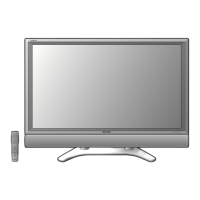
LC-65D90U
∫ IC4001/IC4004 (IXB001WJ)
These ICs are for picture quality correction and left/right split processing.
i) De-contouring: Reduces disturbing noises such as false contours.
ii) LUT system γ correction: Corrects white balance using LUT system.
iii) Color management: Manages gradation between sub-pixels for data outputs.
iv) Advanced BDE: Displays 10-bit quality images on 8-bit panels.
v) Left/right split processing: Selects video data, destined for the QS (Quick Shoot) driver, depending on the
panel setup status.
The input signals consist of dual-link LVDS (RGB, 8 bits each), whereas the output signals are composed of
CMOS (RGB, 8 bits each). Also the sync signal (H,V,DE) which gets in sync with the input signal as well as the
free-running signal (H,V,DE) are output from these ICs. IC4001 and IC4004 serve to give the right-hand and
left-hand video data, respectively, when viewed from the panel front.
∫ IC4003 (IXA998WJ)
The EEPROM stores the 10-bit gamma correction data and crosstalk correction data. When the unit gets
started, the data are read onto the IXB001WJ. (The master IC is IC4004.)
∫ IC4101/IC4201 (IXB002WJ)
The QS (Quick Shoot) driver receives the signals from the picture quality correction and left/right split processing
ICs, and QS-drives them according to the temperature parameter settings of the monitor microprocessor.
LVDS is then activated to give out two lines of signals (for the top LCD controller and the bottom LCD controller).
The control of operational FIFO ICs(IC4102, IC4202:RH-IXA986WJZZQ)is also taken care of here.
IC4101 and IC4201 serve to give the right-hand and left-hand video data, respectively, when viewed from the
panel front.
∫ IC4102/IC4202 (IXA986WJ)
The 26M-bit FIFO ICs work as the QS operational memory.
∫ IC4103/IC4203 (IXB442WJ)
This is a QS parameter storage EEPROM. The data are read frame by frame into the QS driver.
∫ IC4303/IC4903/IC6303/IC6403 (IXA990WJ)
The LCD controller functions like this. The LVDS RGB signals are received from the QS driver (left screen and
right screen) and fed to the FIFO ICs (IC4308, IC4908, IC6308, IC6408: RH-IXA986WJZZQ), as a frame
memory, for top/bottom split processing. The resulting video signals (RSDS) are output to the LCD panel.
IC4303, IC4903, IC4303 and IC6403 serve to give the upper right, upper left, lower right and lower left video
data, respectively, when viewed from the panel front. The control signals for dimmer circuit and CS circuit are
also generated in these ICs. IC4303 is connected with such circuits.
∫ IC4401 (IXB472WJ)
This IC identifies the sync signals and gives out the CS (Chip Select) signal.
With the monitor in the independent mode, the input signal is counted by this IC to identify its synchronization:
i) No sync, ii) 1080p, iii) VGA and iv) Others. Major ICs are under the 3-wire serial control. The CS (Chip
Select) signal for these ICs is generated by this IC.
∫ IC4501/IC6601(BD8133FV)
These ICs have a 19-circuit FET output to supply TFT LCD gradation reference power. The 16 circuits are
used as gradation power, whereas the 2 circuits are employed to control the CS amplitude voltage.
FUNCTIONS OF MAJOR ICs (MONITOR)