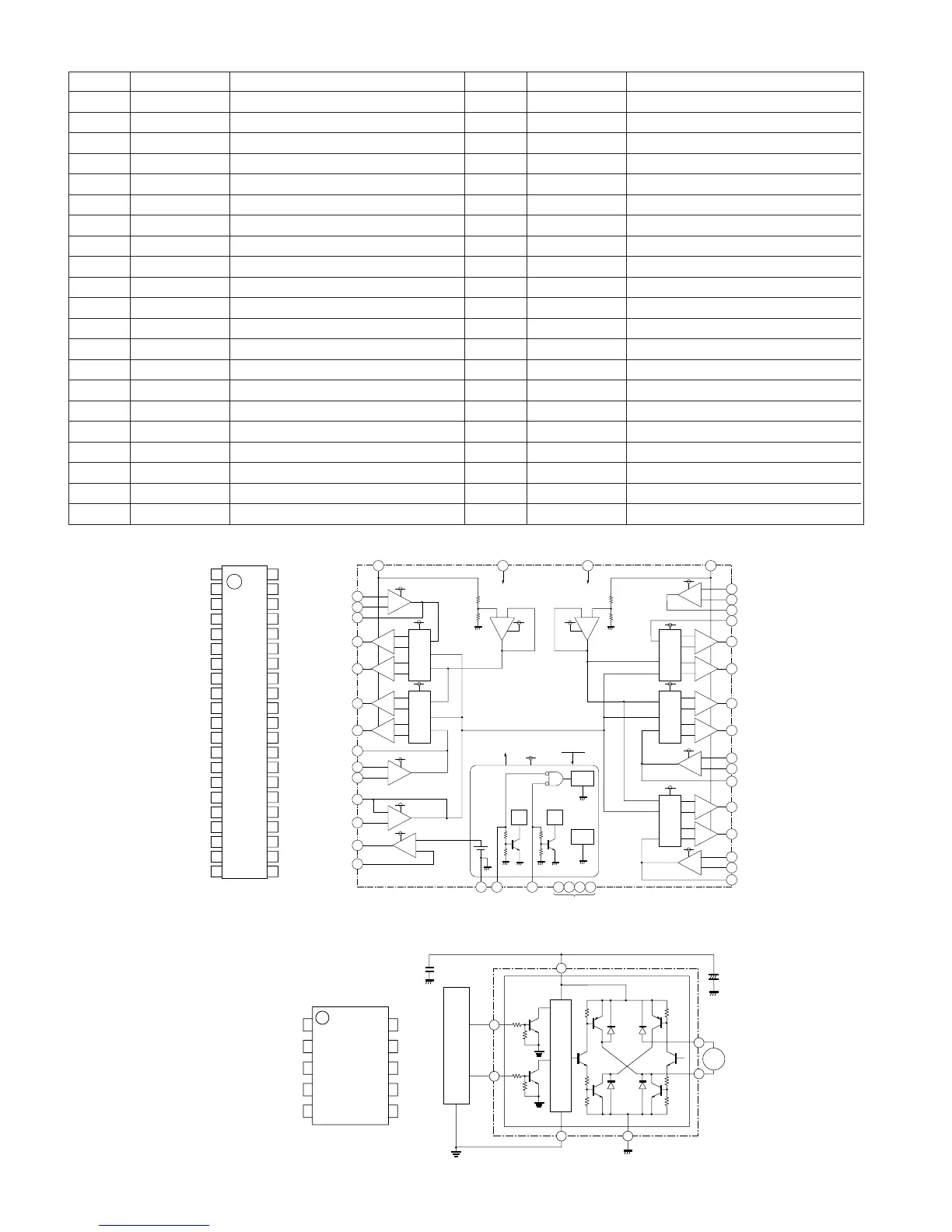
MD-C2
– 94 –
1 CH3IN CH3 non-inverted input
2 OUT3 E3 amplifier output
3 IN3- E3 amplifier inverted input
4 VBS2 Bootstrap power supply
5 Vm2 Motor power supply
6 N.C N.C
7 GND Motor GND
8 IN3+ E3 amplifier non-inverted input
9 VM3- CH3 inverted output
10 VM3+ CH3 non-inverted output
11 GND Motor GND
12 VM4+ CH4 non-inverted output
13 VM4- CH4 inverted output
14 VM5+ CH5 non-inverted output
15 VM5- CH5 inverted output
16 OUT5 E5 amplifier output
17 IN5- E5 amplifier inverted input
18 IN5+ E5 amplifier non-inverted input
19 IN4+ E4 amplifier non-inverted input
20 IN4- E4 amplifier inverted input
21 OUT4 E4 amplifier output
22 VREFO Reference voltage output
23 VREF Reference voltage input
24 SS.GND Small signal GND
25 MUTE2 CH5 mute
26 MUTE1 CH1~4 mute
27 IN2+ E2 amplifier non-inverted input
28 IN2- E2 amplifier inverted input
29 GND Motor GND
30 OUT2 E2 amplifier output
31 VM2- CH2 inverted output
32 VM2+ CH2 non-inverted output
33 GND Motor GND
34 VM1+ CH1 non-inverted output
35 VM1- CH1 inverted output
36 OUT1 E1 amplifier output
37 IN1- E1 amplifier inverted input
38 Vm1 Motor power supply
39 VBS1 Bootstrap power supply
40 IN1+ E1 amplifier non-inverted input
41 REGB Regulator PNP base connect
42 REG+ Regulator voltage setting resistor
IC1601 VHiM56788FP-1:Motor Driver (M56788FP)
Pin No.
Function
Terminal Name
In this unit, the terminal with asterisk mark (*) is (open) terminal which is not connected to the outside.
Pin No.
Function
Terminal Name
1
CH3IN
2
OUT3
3
IN3-
4
VBS2
5
Vm2
6
N.C
7
GND
IN3+
VM3-
VM3+
GND
VM4+
VM4-
VM5+
M56788FP
38
VBS1
IN1+
IN1-
OUT1
VM1+
VM1-
VM2+
VM2-
OUT2
IN2-
IN2+
VREFO
VREF
REGB
REG+
R
R
R
R
E1
E2
VBS1
Vm1
Vm2
Vrefm1
Vrefm2
VREFO
VBS1
39 4
34
36
37
40
+
–
VBS1
27
22
23
41
42
24 26
1.25V
1~4
CH
Low, Open
MUTE ON
28
+
–
VBS1
VBS2
VREF
VREG
–
8
9
10
12
13
13
14
15
VM5-
16
OUT5
17
IN5-
18
IN5+
19
IN4+
20
IN4-
21
42
41
40
39
38
37
36
35
34
33
32
31
30
29
28
27
26
25
24
23
22
OUT4
REG+
REGB
IN1+
VBS1
Vm1
IN1-
OUT1
IN2-
IN2+
MUTE1
MUTE2
SS.GND
VREF
VM1+
VM1-
GND
VM2+
VM2-
OUT2
GND
VREFO
+
–
35
+
–
CH1
x5
32
31
30
10
2
1
8
3
5
19
21
14
15
20
9
12
13
CH2
x5
+
–
+
+
–
VBS2
VBS2
VBS2
VBS2
VBS2
VBS2
E4
E5
E3
–
+
+
–
18
16
17
–
+
+
–
+
–
+
–
CH3
x8
CH4
x8
–
+
–
+
+
–
–
+
+
–
CH5
x8
25 7 112933
5CH
SLEEP
VBS1
BIAS
Hi:Sleep
TSD
SS.GND MUTE1 MUTE2
GND
OUT5
IN5+
IN5-
VM5-
VM5+
OUT4
IN4+
IN4-
VM4-
VM4+
VM3-
VM3+
CH3IN
OUT3
IN3+
IN3-
Vm2VBS2VBS1Vm1
+
–
IC1602 VHiLB1930M/-1: Motor Driver (LB1930M)
VCC
1
2
3
4
5
10
9
8
7
6
NC
IN 1
IN 2
S–GND
NC
OUT 1
NC
OUT 2
P–GND
IN2
OUT2
OUT1
C1=IµF
M
IN1
60K
80K
60K
80K
CPU
CONTROLLER
S–GND
P–GND
VCC
1
3
4
5 6
7
9
Figure 94-2 BLOCK DIAGRAM OF IC
Figure 94-1 BLOCK DIAGRAM OF IC